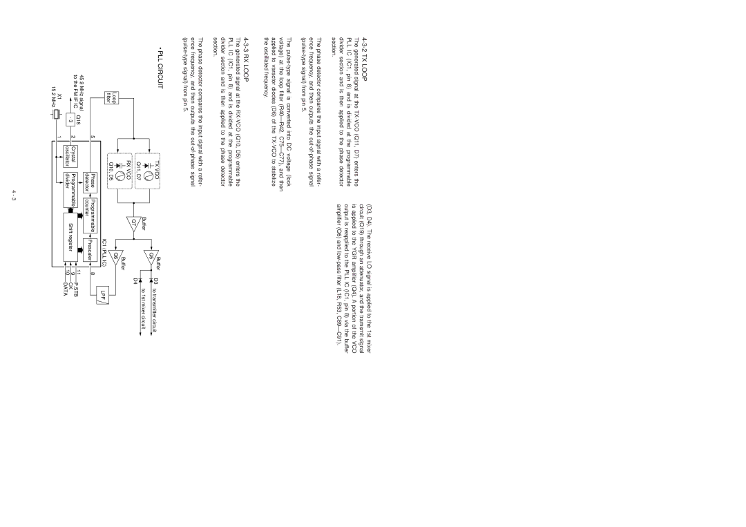
4-3 PLL CIRCUIT
4-3-1 GENERAL
A PLL circuit provides stable oscillation of the transmit fre- quency and receive 1st LO frequency. The PLL output com- pares the phase of the divided VCO frequency to the refer- ence frequency. The PLL output frequency is controlled by a crystal oscillator and the divided ratio
The PLL circuit, using a one chip PLL IC (IC1), directly gen- erates the transmit frequency and divided ratio based on serial data from the CPU and compares the phases of VCO signals with the reference oscillator frequency. The PLL IC detects the
4-3-2 TX LOOP
The generated signal at the
The phase detector compares the input signal with a refer- ence frequency, and then outputs the
The
4-3-3 RX LOOP
The generated signal at the
The phase detector compares the input signal with a refer- ence frequency, and then outputs the
The
4-3-4 VCO CIRCUIT
The VCO outputs from Q11 (TX) and Q10 (RX) are buffer amplified at Q7 and Q6, and are then sent to the T/R switch (D3, D4). The receive LO signal is applied to the 1st mixer circuit (Q19) through an attenuator, and the tramsmit signal is applied to the YGR amplifier (Q4). A portion of the VCO output is reapplied to the PLL IC (IC1, pin 8) via the buffer amplifier (Q6) and
 PLL CIRCUIT
Loop
filter
45.9 MHz signal Q18 to the FM IF IC
⋅3
X1
15.2 MHz
TX VCO | Buffer | D3 | to transmitter circuit | |
Q5 | ||||
|
|
| ||
Buffer |
|
| to 1st mixer circuit | |
Q11, D7 |
| D4 |
| |
Q7 |
|
| ||
|
|
|
RX VCO
Buffer
![]() Q6
Q6
| Q10, D5 |
|
|
|
|
| ||
|
|
|
|
| IC1 (PLL IC) |
| LPF | |
|
|
|
|
|
|
| ||
5 |
| Phase | Programmable | Prescaler | 8 |
| ||
|
| detector | counter |
|
|
| ||
|
|
|
|
|
| |||
2 | Crystal | Programmable |
|
| 11 | P.STB | ||
Shift register | 9 | |||||||
CK | ||||||||
| oscillator | divider |
| 10 | ||||
|
|
|
| DATA | ||||
|
|
|
|
|
|
| ||
1 |
|
|
|
|
|
|
| |
4 - 3