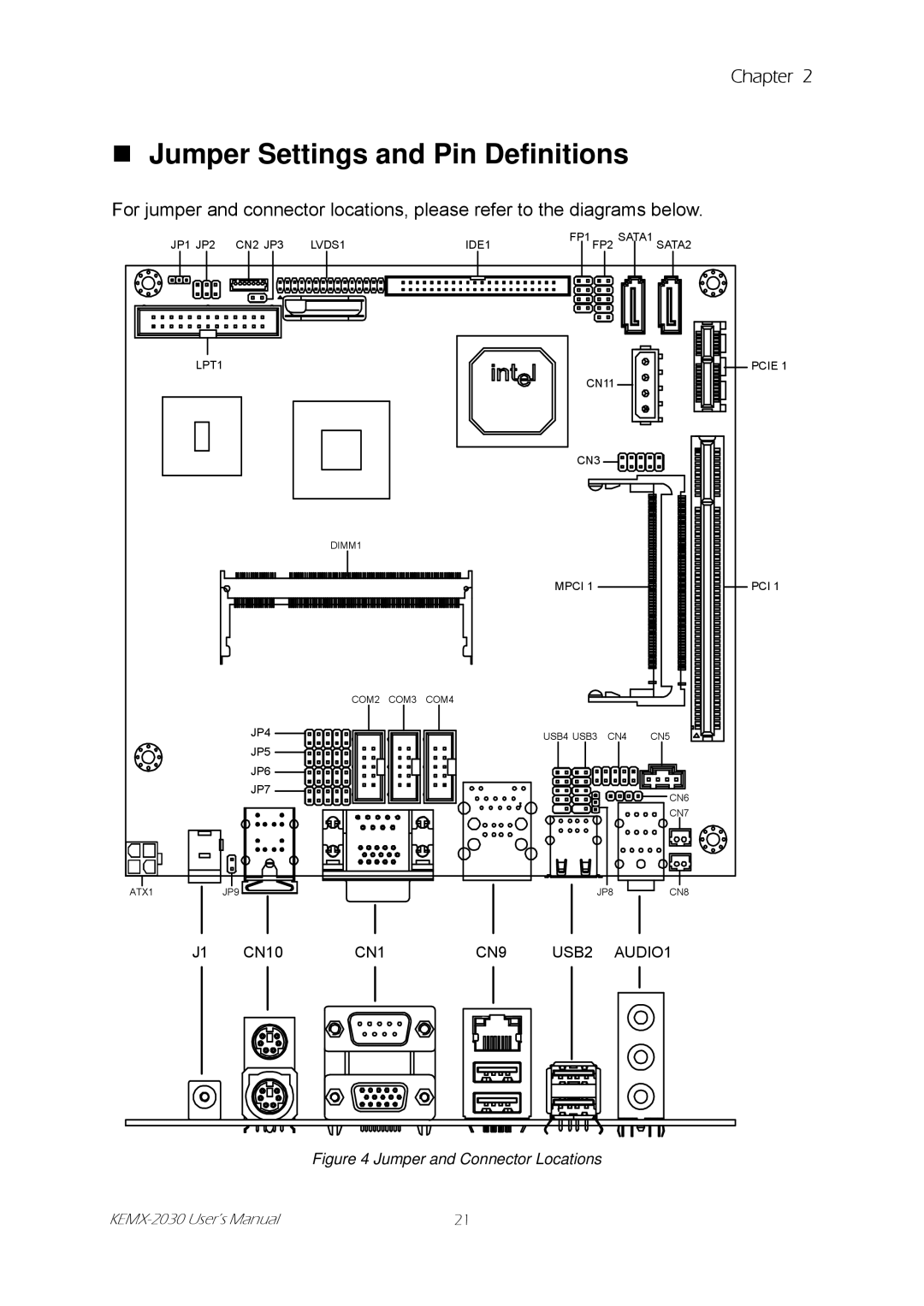
KEMX-2030 specifications
The Intel KEMX-2030 is a cutting-edge processor designed to push the boundaries of performance and efficiency in computing applications. This innovative chip integrates advanced technologies that cater to a variety of users, from gamers to data scientists, ensuring that it meets the demands of modern workloads.At the heart of the KEMX-2030 is Intel's latest microarchitecture, which enhances instruction execution and optimizes power consumption. This microarchitecture employs a combination of high-performance cores and energy-efficient cores, allowing for dynamic scaling based on workload requirements. This enables the KEMX-2030 to deliver exceptional performance while maintaining energy efficiency, a crucial factor in today's environmentally conscious world.
One of the standout features of the KEMX-2030 is its support for Intel's Hyper-Threading technology. This technology allows each core to handle two threads simultaneously, effectively doubling the number of tasks the processor can manage at once. As a result, users can experience improved multitasking and faster processing times, especially in applications that require heavy computations.
The KEMX-2030 also includes built-in artificial intelligence (AI) capabilities that facilitate real-time machine learning applications. With dedicated AI accelerators, the processor can efficiently execute complex algorithms, making it suitable for tasks such as image and speech recognition, natural language processing, and more. This integration of AI and machine learning technologies not only boosts productivity but also opens up new avenues for innovation across industries.
In terms of connectivity, the KEMX-2030 supports the latest standards, including Thunderbolt 4 and USB4. This enables high-speed data transfers and connectivity to a wide array of peripherals. Additionally, the processor is optimized for use in edge computing environments, making it an ideal choice for IoT applications that require quick and reliable data processing at the source.
Thermal management is another critical aspect of the KEMX-2030's design. The processor utilizes advanced thermal throttling techniques to regulate temperature effectively during intensive tasks. This ensures stable performance without the risk of overheating, prolonging the lifespan of the hardware.
In summary, the Intel KEMX-2030 represents a significant advancement in processor technology. With its high-performance capabilities, energy-efficient design, and robust support for AI and connectivity, it is poised to become a preferred choice for a wide range of computing applications, driving innovation and efficiency in various fields.

