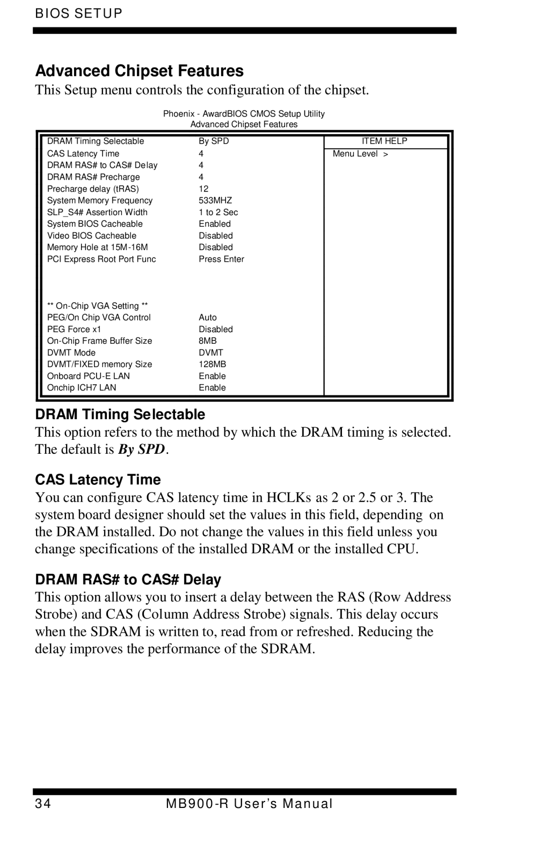
MB900-R specifications
The Intel MB900-R is an advanced embedded microcontroller designed for a variety of applications that require high performance, low power consumption, and robust connectivity options. Specifically built to cater to the needs of industrial automation, motor control, and IoT devices, the MB900-R series boasts a range of features that enhance its versatility and usability.One of the standout characteristics of the MB900-R is its powerful multi-core architecture. It often integrates several cores, enabling it to handle simultaneous tasks efficiently. This feature is particularly beneficial in applications that require real-time processing and quick responsiveness.
The device is built on Intel's modern manufacturing processes, which ensure exceptional energy efficiency. This makes the MB900-R suitable for battery-operated devices and applications where power conservation is critical. Its low thermal output contributes to reliability, even under heavy loads, which is essential for long-term deployment in industrial environments.
In terms of connectivity, the MB900-R offers a variety of interfaces, including SPI, I2C, UART, and Ethernet. Such capabilities facilitate seamless integration with numerous sensors and other peripherals, making it highly adaptable to different use cases. Furthermore, the microcontroller supports various wireless communication protocols, such as Bluetooth and Wi-Fi, enabling developers to create connected applications for the Internet of Things.
Moreover, the MB900-R series includes advanced security features, which are increasingly important in today’s connected landscape. With built-in encryption and secure boot processes, the device ensures data integrity and protection against unauthorized access, catering to sectors where data security is paramount.
The robust toolchain and software compatibility provided by Intel makes it easier for developers to create, debug, and deploy applications quickly. With support for multiple programming languages and development environments, the MB900-R allows for flexibility in coding, ensuring that developers can utilize the best tools for their specific needs.
Overall, the Intel MB900-R microcontroller exemplifies cutting-edge design and technology in embedded systems, making it an ideal choice for a wide range of high-performance, low-power applications across industries, including automotive, industrial, and consumer electronics. Its efficient architecture, extensive connectivity options, security features, and developer-friendly ecosystem position it as a vital component in the smart devices of tomorrow.
