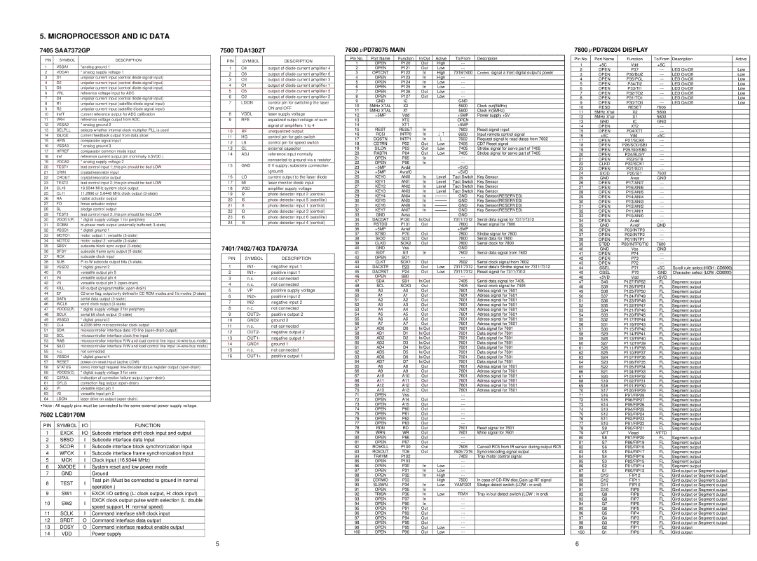
5. MICROPROCESSOR AND IC DATA
7405 SAA7372GP
PIN | SYMBOL | DESCRIPTION |
|
|
|
1 | VSSA1 | *analog ground 1 |
|
|
|
2 | VDDA1 | * analog supply voltage 1 |
3 | D1 | unipolar current input (central diode signal input) |
|
|
|
4 | D2 | unipolar current input (central diode signal input) |
5 | D3 | unipolar current input (central diode signal input) |
|
|
|
6 | VRL | reference voltage input for ADC |
7 | D4 | unipolar current input (central diode signal input) |
8 | R1 | unipolar current input (satellite diode signal input) |
|
|
|
9 | R2 | unipolar current input (satellite diode signal input) |
10 | IrefT | current reference output for ADC calibration |
|
|
|
11 | VRH | reference voltage output from ADC |
12 | VSSA2 | * analog ground 2 |
|
|
|
13 | SELPLL | selects whether internal clock multiplier PLL is used |
14 | ISLICE | current feedback output from data slicer |
|
|
|
15 | HFIN | comparator signal input |
16 | VSSA3 | * analog ground 3 |
|
|
|
17 | HFREF | comparator common mode input |
18 | Iref | reference current output pin (nominally 0.5VDD ) |
19 | VDDA2 | * analog supply voltage 2 |
|
|
|
20 | TEST1 | test control input 1; this pin should be tied LOW |
21 | CRIN | crystal/resonator input |
22 | CROUT | crystal/resonator output |
23 | TEST2 | test control input 2; this pin should be tied LOW |
24 | CL16 | 16.9344 MHz system clock output |
25 | CL11 | 11.2896 or 5.6448 MHz clock output |
26 | RA | radial actuator output |
27 | FO | focus actuator output |
28 | SL | sledge control output |
29 | TEST3 | test control input 3; this pin should be tied LOW |
30 | VDDD1(P) | * digital supply voltage 1 for periphery |
31 | DOBM | |
32 | VSSD1 | * digital ground 1 |
33 | MOTO1 | motor output 1; versatile |
34 | MOTO2 | motor output 2; versatile |
35 | SBSY | subcode block sync output |
36 | SFSY | subcode frame sync output |
|
|
|
37 | RCK | subcode clock input |
38 | SUB | |
|
|
|
39 | VSSD2 | * digital ground 2 |
40 | V5 | versatile output pin 5 |
|
|
|
41 | V4 | versatile output pin 4 |
42 | V3 | versatile output pin 3 |
43 | KILL | kill output (programmable; |
|
|
|
44 | EF | C2 error flag; output only defined in CD ROM modes and 1fs modes |
45 | DATA | serial data output |
46 | WCLK | word clock output |
47 | VDDD2(P) | * digital supply voltage 2 for periphery |
48 | SCLK | serial bit clock output |
49 | VSSD3 | * digital ground 3 |
|
|
|
50 | CL4 | 4.2336 MHz microcontroller clock output |
51 | SDA | microcontroller interface data I/O line |
|
|
|
52 | SCL | microcontroller interface clock line input |
53 | RAB | microcontroller interface R/W and load control line input |
54 | SILD | microcontroller interface R/W and load control line input |
55 | n.c. | not connected |
56 | VSSD4 | * digital ground 4 |
|
|
|
57 | RESET | |
58 | STATUS | servo interrupt request line/decoder status register output |
|
|
|
59 | VDDD3(C) | * digital supply voltage 3 for core |
60 | C2FAIL | indication of correction failure output |
|
|
|
61 | CFLG | correction flag output |
62 | V1 | versatile input pin 1 |
63 | V2 | versatile input pin 2 |
64 | LDON | laser drive on output |
![]() Note : All supply pins must be connected to the same external power supply voltage.
Note : All supply pins must be connected to the same external power supply voltage.
7602 LC89170M
PIN | SYMBOL | I/O | FUNCTION | |
|
|
|
| |
1 | EXCK | I/O | Subcode interface shift clock input and output | |
2 | SBSO | I | Subcode interface data Input | |
3 | SCOR | I | Subcode interface block synchronization Input | |
4 | WFCK | I | Subcode interface frame synchronization Input | |
5 | MCK | I | Clock input (16.9344 MHz) | |
6 | XMODE | I | System reset and low power mode | |
7 | GND |
| Ground | |
8 | TEST | I | Test pin (Must be connected to ground in normal | |
operation.) | ||||
|
|
| ||
9 | SW1 | I | EXCK I/O setting (L: clock output, H: clock input) | |
10 | SW2 | I | EXCK clock output pulse width selection (L: double | |
speed support, H: normal speed) | ||||
|
|
| ||
11 | SCLK | I | Command interface shift clock input | |
12 | SRDT | O | Command interface data output | |
13 | DOSY | O | Command interface readout enable output | |
14 | VDD |
| Power supply |
7500 TDA1302T
PIN | SYMBOL | DESCRIPTION |
|
|
|
1 | O4 | output of diode current amplifier 4 |
|
|
|
2 | O6 | output of diode current amplifier 6 |
3 | O3 | output of diode current amplifier 3 |
|
|
|
4 | O1 | output of diode current amplifier 1 |
5 | O5 | output of diode current amplifier 5 |
|
|
|
6 | O2 | output of diode current amplifier 2 |
7 | LDON | control pin for switching the laser |
|
| ON and OFF |
|
|
|
8 | VDDL | laser supply voltage |
|
|
|
9 | RFE | equalized output voltage of sum |
|
| signal of amplifiers 1 to 4 |
10 | RF | unequalized output |
|
|
|
11 | HG | control pin for gain switch |
12 | LS | control pin for speed switch |
|
|
|
13 | CL | external capacitor |
14 | ADJ | reference input normally |
|
| connected to ground via a resistor |
15 | GND | 0 V supply; substrate connection |
|
| (ground) |
16 | LO | current output to the laser diode |
|
|
|
17 | MI | laser monitor diode input |
18 | VDD | amplifier supply voltage |
19 | I2 | photo detector input 2 (central) |
|
|
|
20 | I5 | photo detector input 5 (satellite) |
21 | I1 | photo detector input 1 (central) |
|
|
|
22 | I3 | photo detector input 3 (central) |
23 | I6 | photo detector input 6 (satellite) |
|
|
|
24 | I4 | photo detector input 4 (central) |
7401/7402/7403 TDA7073A
PIN | SYMBOL | DESCRIPTION |
|
|
|
1 | IN1- | negative input 1 |
2 | IN1+ | positive input 1 |
3 | n.c. | not connected |
4 | n.c. | not connected |
5 | VP | positive supply voltage |
6 | IN2+ | positive input 2 |
7 | IN2- | negative input 2 |
|
|
|
8 | n.c. | not connected |
9 | OUT2+ | positive output 2 |
10 | GND2 | ground 2 |
11 | n.c. | not connected |
12 | OUT2- | negative output 2 |
13 | OUT1- | negative output 1 |
14 | GND1 | ground 1 |
15 | n.c. | not connected |
16 | OUT1+ | positive output 1 |
|
|
|
7600  PD78076 MAIN
Pin No. | Port Name | Function | In/Out |
| Active |
| To/From | Description |
1 | OPEN | P120 | Out |
| High |
|
| |
2 | OPEN | P121 | Out |
| Low |
|
| |
3 | OPTCNT | P122 | In |
| High |
| 7318/7400 | Control signal a front digital output's power |
4 | OPEN | P123 | In |
| High |
|
| |
5 | OPEN | P124 | In |
| Low |
|
| |
6 | OPEN | P125 | In |
| Low |
|
| |
7 | OPEN | P126 | Out |
| Low |
|
| |
8 | OPEN | P127 | Out |
| Low |
|
| |
9 | GND | IC |
|
|
|
| GND |
|
10 | 5MHz XTAL | X2 |
|
|
|
| 5600 | Clock out(5MHz) |
11 | 5MHz XTAL | X1 |
|
|
|
| 5600 | Clock in(5MHz) |
12 | +5MP | Vdd |
|
|
|
| +5MP | Power supply +5V |
13 |
| XT2 |
|
|
|
| OPEN |
|
14 |
| XT1 |
|
|
|
| +5MP |
|
15 | REST | RESET | In |
|
|
| 7603 | Reset signal input |
16 | RC5I | INTP0 | In |
|
|
| 6600 | Input remote control signal |
17 | DQSTN | INTP1 | In |
|
|
| 7602 | Request signal to read datas from 7602 |
18 | CD7RN | P02 | Out |
| Low |
| 7405 | CD7 Reset signal |
19 | SILDN | P03 | Out |
| Low |
| 7405 | Strobe signal for servo part of 7405 |
20 | RAB7N | P04 | Out |
| Low |
| 7405 | Strobe signal for servo part of 7405 |
21 | OPEN | P05 | In |
|
|
|
| |
22 | OPEN | P06 | In |
|
|
|
| |
23 | +5MP | Avdd |
|
|
|
| +5VD |
|
24 | +5MP | Avref0 |
|
|
|
| +5VD |
|
25 | KEY0 | ANI0 | In |
| Level |
| Tact Switch | Key Sensor |
26 | KEY1 | ANI1 | In |
| Level |
| Tact Switch | Key Sensor |
27 | KEY2 | ANI2 | In |
| Level |
| Tact Switch | Key Sensor |
28 | KEY3 | ANI3 | In |
| Level |
| Tact Switch | Key Sensor |
29 | KEY4 | ANI4 | In |
|
|
| GND | Key Sensor(RESERVED) |
| ||||||||
30 | KEY5 | ANI5 | In |
|
|
| GND | Key Sensor(RESERVED) |
| ||||||||
31 | KEY6 | ANI6 | In |
|
|
| GND | Key Sensor(RESERVED) |
| ||||||||
32 | KEY7 | ANI7 | In |
|
|
| GND | Key Sensor(RESERVED) |
| ||||||||
33 | GND | Avss |
|
|
|
| GND |
|
34 | DACDAT | P130 | In/Out |
|
|
| 7311/7312 | Serial data signal for 7311/7312 |
35 | RSTDD | P131 | Out |
|
|
| 7800 | Reset signal for 7800 |
36 | +5MP | Avref |
|
|
|
| +5MP |
|
37 | STBD | P70 | Out |
|
|
| 7800 | Strobe signal for 7800 |
38 | SIOD | SO2 | Out |
|
|
| 7800 | Serial data for 7800 |
39 | CLKD | SCK2 | Out |
|
|
| 7800 | Serial clock for 7800 |
40 | GND | Vss |
|
|
|
| GND |
|
41 | SIDT | SI1 | In |
|
|
| 7602 | Serial data signal from 7602 |
42 | OPEN | SO1 |
|
|
|
|
| |
43 | CLKT | SCK1 | Out |
|
|
| 7602 | Serial clock signal from 7602 |
44 | DACSTR | P23 | Out |
| Low |
| 7311/7312 | Serial data's Strobe signal for 7311/7312 |
45 | DACRST | P24 | Out |
| Low |
| 7311/7312 | Reset signal for 7311/7312 |
46 | OPEN | SB0 |
|
|
|
|
| |
47 | SDA | SB1 | In/Out |
|
|
| 7405 | Serial data signal for 7405. |
48 | SCL | SCK0 | Out |
|
|
| 7405 | Serial clock signal for 7405 |
49 | A0 | A0 | Out |
|
|
| 7601 | Adress signal for 7601 |
50 | A1 | A1 | Out |
|
|
| 7601 | Adress signal for 7601 |
51 | A2 | A2 | Out |
|
|
| 7601 | Adress signal for 7601 |
52 | A3 | A3 | Out |
|
|
| 7601 | Adress signal for 7601 |
53 | A4 | A4 | Out |
|
|
| 7601 | Adress signal for 7601 |
54 | A5 | A5 | Out |
|
|
| 7601 | Adress signal for 7601 |
55 | A6 | A6 | Out |
|
|
| 7601 | Adress signal for 7601 |
56 | A7 | A7 | Out |
|
|
| 7601 | Adress signal for 7601 |
57 | AD0 | D0 | In/Out |
|
|
| 7601 | Data signal for 7601 |
58 | AD1 | D1 | In/Out |
|
|
| 7601 | Data signal for 7601 |
59 | AD2 | D2 | In/Out |
|
|
| 7601 | Data signal for 7601 |
60 | AD3 | D3 | In/Out |
|
|
| 7601 | Data signal for 7601 |
61 | AD4 | D4 | In/Out |
|
|
| 7601 | Data signal for 7601 |
62 | AD5 | D5 | In/Out |
|
|
| 7601 | Data signal for 7601 |
63 | AD6 | D6 | In/Out |
|
|
| 7601 | Data signal for 7601 |
64 | AD7 | D7 | In/Out |
|
|
| 7601 | Data signal for 7601 |
65 | A8 | A8 | Out |
|
|
| 7601 | Adress signal for 7601 |
66 | A9 | A9 | Out |
|
|
| 7601 | Adress signal for 7601 |
67 | A10 | A10 | Out |
|
|
| 7601 | Adress signal for 7601 |
68 | A11 | A11 | Out |
|
|
| 7601 | Adress signal for 7601 |
69 | A12 | A12 | Out |
|
|
| 7601 | Adress signal for 7601 |
70 | A13 | A13 | Out |
|
|
| 7601 | Adress signal for 7601 |
71 | OPEN | Vss |
|
|
|
|
| |
72 | OPEN | A14 | Out |
|
|
|
| |
73 | OPEN | A15 | Out |
|
|
|
| |
74 | OPEN | P60 | Out |
|
|
|
| |
75 | OPEN | P61 | Out |
|
|
|
| |
76 | OPEN | P62 | Out |
|
|
|
| |
77 | OPEN | P63 | Out |
|
|
|
| |
78 | RDN | RD | Out |
|
|
| 7601 | Read signal for 7601 |
79 | WRN | WR | Out |
|
|
| 7601 | Write signal for 7601 |
80 | OPEN | P66 | Out |
|
|
|
| |
81 | OPEN | P67 | Out |
|
|
|
| |
82 | RC5KILL | P100 | Out |
|
|
| 7605 | Cancell RC5 from IR sensor during output RC5 |
83 | RC5OUT | TO6 | Out |
|
|
| 7605/7316 | Syncrorecoding signal output |
84 | TRAYM | P102 |
|
|
|
| 7403 | Tray motor control signal |
85 | OPEN | P103 |
|
|
|
|
| |
86 | OPEN | P30 | In |
| Low |
|
| |
87 | OPEN | P31 | In |
| Low |
|
| |
88 | OPEN | P32 | In |
| High |
|
| |
89 | CDRWO | P33 |
|
| High |
| 7500 | In case of |
90 | SLSWN | P34 | In |
| Low |
| VAM1201 | Sledge detect switch (LOW : in end) |
91 | OPEN | P35 | In |
|
|
|
| |
92 | TRISN | P36 | In |
| Low |
| TRAY | Tray in/out detect switch (LOW : in end) |
93 | OPEN | P37 | In |
|
|
|
| |
94 | OPEN | P90 | In |
|
|
|
| |
95 | OPEN | P91 | Out |
|
|
|
| |
96 | OPEN | P93 | Out |
|
|
|
| |
97 | OPEN | P94 | Out |
|
|
|
| |
98 | OPEN | P95 | Out |
|
|
|
| |
99 | OPEN | P95 | Out |
| Low |
|
| |
100 | OPEN | P96 | Out |
| Low |
|
|
7800 | PD780204 DISPLAY |
|
|
| |
Pin No. | Port Name | Function | To/From | Description | Active |
|
|
|
|
|
|
1 | +5C | Vdd | +5C |
|
|
2 | OPEN | P37 | LED On/Off | Low | |
3 | OPEN | P36/BUZ | LED On/Off | Low | |
4 | OPEN | P35/PCL | LED On/Off | Low | |
5 | OPEN | P34/TI2 | LED On/Off | Low | |
6 | OPEN | P33/TI1 | LED On/Off | Low | |
7 | OPEN | P32/TO2 | LED On/Off | Low | |
8 | OPEN | P31/TO1 | LED On/Off | Low | |
9 | OPEN | P30/TO0 | LED On/Off | Low | |
10 | RESD | RESET | 7600 |
|
|
11 | 5MHz X’tal | X2 | 5800 |
|
|
12 | 5MHz X’tal | X1 | 5800 |
|
|
13 | GND | IC | GND |
|
|
14 | OPEN | XT2 |
|
| |
15 | OPEN | P04/XT1 |
|
| |
16 | +5C | Vdd | +5C |
|
|
17 | OPEN | P27/SCK0 |
|
| |
18 | OPEN | P26/SO0/SB1 |
|
| |
19 | OPEN | P25/SI0/SB0 |
|
| |
20 | OPEN | P24/BUSY |
|
| |
21 | OPEN | P23/STB |
|
| |
22 | CLKD | P22/SCK1 |
|
| |
23 | OPEN | P21/SO1 |
|
| |
24 | SIOD | P20/SI1 | 7600 |
|
|
25 | GND | Avss | GND |
|
|
26 | OPEN | P17/ANI7 |
|
| |
27 | OPEN | P16/ANI6 |
|
| |
28 | OPEN | P15/ANI5 |
|
| |
29 | OPEN | P14/ANI4 |
|
| |
30 | OPEN | P13/ANI3 |
|
| |
31 | OPEN | P12/ANI2 |
|
| |
32 | OPEN | P11/ANI1 |
|
| |
33 | OPEN | P10/ANI0 |
|
| |
34 | OPEN | Avdd |
|
| |
35 | GND | Avref | GND |
|
|
36 | OPEN | P03/INTP3 |
|
| |
37 | OPEN | P02/INTP2 |
|
| |
38 | OPEN | P01/INTP1 |
|
| |
39 | STBD | P00/INTP0/TI0 | 7600 |
|
|
40 | GND | Vss | GND |
|
|
41 | OPEN | P74 |
|
| |
42 | OPEN | P73 |
|
| |
43 | OPEN | P72 |
|
| |
44 | SSEL | P71 | +5C | Scroll rule select (HIGH : CD6000) |
|
45 | CSEL | P70 | GND | Character select (LOW : CD6000) |
|
46 | +5VD | Vdd | +5VD |
|
|
47 | S40 | P127/FIP52 | FL | Segment output |
|
48 | S39 | P126/FIP51 | FL | Segment output |
|
49 | S38 | P125/FIP50 | FL | Segment output |
|
50 | S37 | P124/FIP49 | FL | Segment output |
|
51 | S36 | P123/FIP48 | FL | Segment output |
|
52 | S35 | P122/FIP47 | FL | Segment output |
|
53 | S34 | P121/FIP46 | FL | Segment output |
|
54 | S33 | P120/FIP45 | FL | Segment output |
|
55 | S32 | P117/FIP44 | FL | Segment output |
|
56 | S31 | P116/FIP43 | FL | Segment output |
|
57 | S30 | P115/FIP42 | FL | Segment output |
|
58 | S29 | P114/FIP41 | FL | Segment output |
|
59 | S28 | P113/FIP40 | FL | Segment output |
|
60 | S27 | P112/FIP39 | FL | Segment output |
|
61 | S26 | P111/FIP38 | FL | Segment output |
|
62 | S25 | P110/FIP37 | FL | Segment output |
|
63 | S24 | P107/FIP36 | FL | Segment output |
|
64 | S23 | P106/FIP35 | FL | Segment output |
|
65 | S22 | P105/FIP34 | FL | Segment output |
|
66 | S21 | P104/FIP33 | FL | Segment output |
|
67 | S20 | P103/FIP32 | FL | Segment output |
|
68 | S19 | P102/FIP31 | FL | Segment output |
|
69 | S18 | P101/FIP30 | FL | Segment output |
|
70 | S17 | P100/FIP29 | FL | Segment output |
|
71 | S16 | P97/FIP28 | FL | Segment output |
|
72 | S15 | P96/FIP27 | FL | Segment output |
|
73 | S14 | P95/FIP26 | FL | Segment output |
|
74 | S13 | P94/FIP25 | FL | Segment output |
|
75 | S12 | P93/FIP24 | FL | Segment output |
|
76 | S11 | P92/FIP23 | FL | Segment output |
|
77 | S10 | P91/FIP22 | FL | Segment output |
|
78 | S9 | P90/FIP21 | FL | Segment output |
|
79 | Vload |
|
|
| |
80 | S8 | P87/FIP20 | FL | Segment output |
|
81 | S7 | P86/FIP19 | FL | Segment output |
|
82 | S6 | P85/FIP18 | FL | Segment output |
|
83 | S5 | P84/FIP17 | FL | Segment output |
|
84 | S4 | P83/FIP16 | FL | Segment output |
|
85 | S3 | P82/FIP15 | FL | Segment output |
|
86 | S2 | P81/FIP14 | FL | Segment output |
|
87 | S1 | P80/FIP13 | FL | Gird output or Segment output |
|
88 | G13 | FIP12 | FL | Gird output or Segment output |
|
89 | G12 | FIP11 | FL | Gird output or Segment output |
|
90 | G11 | FIP10 | FL | Gird output or Segment output |
|
91 | G10 | FIP9 | FL | Gird output or Segment output |
|
92 | G9 | FIP8 | FL | Gird output or Segment output |
|
93 | G8 | FIP7 | FL | Gird output or Segment output |
|
94 | G7 | FIP6 | FL | Gird output or Segment output |
|
95 | G6 | FIP5 | FL | Gird output or Segment output |
|
96 | G5 | FIP4 | FL | Gird output or Segment output |
|
97 | G4 | FIP3 | FL | Gird output or Segment output |
|
98 | G3 | FIP2 | FL | Gird output or Segment output |
|
99 | G2 | FIP1 | FL | Gird output |
|
100 | G1 | FIP0 | FL | Gird output |
|
5 | 6 |