1 2

A

PWB-FRONT1

B

IN3-Y

GND*

IN3-Pb

GND*

IN3-Pr

GND*

IN3-R

GND*

IN3-L

GND*

YUV-SW

CVBS-SW


1

2

3

4

5

6

7

8

9

10

11

12

CE1

PA-H

C

SHIELD


3


4

5


6


7


8


9


10

11

12

V39 & V39+ only


PWB-LED


PWB-CONT

PWB-PREAMP

PWB-SBL-L PWB-SBL-R


LED-R

LED-G

STATUS-R

STATUS-G

GND LED

KSC0


GND

KSC0

KSC1

SYSTEM/RESET


5VS

IRIN

3.3VSL

RMC

GND

L12V

LRTN

GH-H

R12V

RRTN

GH-H


PA-H

PA-H


PA-H


4

SL

5

4

SR

5


7

6

5

4

3

2

1


4

3

2

1


5

4

3

2

1

1

2

3

1

2

3


LE3


LE2


LE1


PWB-LED2

LED-R

LED-G

-STATUSR

-STATUSG


SMR

KSC0 GND LED

PA-H

SB1


7

6

5

4

3

2

1


SMR


LE4


V39++ only


13

14

15

16

17

PWB-FRONTHDMI


HOTPLUG_DETE

+5V

GND

DDC_SDA

DDC_SCL

NC

CEC

GND

TXC-

TXC+

GND

TX0-

TX0+

GND

TX1-

TX1+

GND

TX2-

TX2+

GND


GND

EDID-SDA

EDID-SCL

GND

CEC


PA


21

20

19

18

17

16

15

14

13

12

11

10

9

8

7

6

5

4

3

2

1


GND 26


G

22

5

4

3

2

1

G


GND


HD1


GND 27

G


FI-RE21S-HF


G

23

GND


HD2


GND

28

G


G

24

GND


GND

29

G


G

25

GND


TMDS CABLE ( FFC type )

18 19

FRONT-USB 3D

CABLE


USB

CABLE-3D

20 21 22

PG 1.....BLOCK

V39-V39++

*NOTES

1.DC voltages were measured from points indicated to the circuit ground with a high-Z voltmeter

2.Wave form were taken with standard color bar signal.

3.TP13.etc. show test points.

4.CAPACITOR

Value

Not indicated PF, for numbers more than 1


uF, for numbers less than 1

Dielectric


strength

Not indicated : 50V


No tolerance is indicated


Not indicated = +/- 10% for electrolytic capacitor

Tolerance


and +/- 20%

G=+/-2%

P=+100%

Q=+30%

C=+/-0.25PF


J=+/-5%

-0%

-10%

D=+/-0.5PF


K=+/-10%

Z=+80%

T=+200%

F=+/-1PF


M=+/-20%

-20%

-0%

D=+/-2PF


Not indicated: Ceramic capacitor


CE


1

2

3

4

5

6

7

8

9

10

11

12

IN3-Y

GND*

IN3-Pb

GND*

IN3-Pr

GND*

IN3-R

GND*

IN3-L

GND*

YUV-SW

CVBS-SW

PA-H


D


MAIN 2


E

F

G


LE


SB


16

15

14

13

12

11

10

9

8

7

6

5

4

3

2

1


1

2

3

4


BOSS


PA-H


PA-H

L12V

LRTN

R12V


-RLED

-GLED

-RSTATUS

-GSTATUS

LED

GND

KSC0

GND

KSC0

KSC1

SYSTEM/RESET

5VS

IRIN

3.3VSL

RMC

GND


MAIN 3

RRTN


MAIN 1


V39++ only

PWB-MAIN

GND 25

G


G

29

GND


3D


GND 24

G


G

28

GND


HD2


US


UB


GND 23

G


FI-RE21S-VF


G

27

GND


1

2

3

4

G

G


HD1


4

3

2

1


GND 22

G


26

GND

5

4

3

2

1


G


DETEHOTPLUG

+5V

GND

SDADDC

SCLDDC

NC

CEC

GND

-TXC

MAIN 3

TX0+

GND

-TX1

TX1+

GND

-TX2

TX2+

GND

SDA-EDID

SCL-EDID

GND

CEC

VCCUSB

D1-

MAIN 5

GND

GND

MAINSYNCSTEREO GND

1


GND


1

2

3

4

5

6

7

8

9

10

TXC+

GND

TX0-

14

15

16

17

18

19

20

21


D1+

GNDUSB

GND


5VDC


11

12

13


PA


PA-H

MAIN 3

V39+ & V39++ only


MF

: Polyester capacitor


PP

: Polypropylene film capacitor


ALM : Aluminus electrolytic capacitor

Parts

TF

: Twin film capacitor


except

SC

: Semiconductor Ceramic capacitor


Type


I for

MP

: Metalized paper

chips

MPP : Metalized plastic film capacitor


MMF : Metalized polyester capacitor


: Polyester polypropylene film


MF,PP

capacitor


PS

: Styrol capacitor


TAN or TANT: Tantalum capacitor


+


: Electrolytic capacitor


NP

: Non polarized electrolytic


capacitor


Not indicated:Ceramic capacitor chip


II chips

+


: Electrolytic capacitor


NP

: Non polarized electrolytic


capacitor chip

Characteristic Not indicated

:

F or B (high dielrctric percentage)

(Only ceramic

CH, SL, etc.


:

Temperature compensaing types

capacitor)


5. RESITOR


Not indicated

=

Ohm


Value


K

=

1,000 Ohm


M

=

1,000,000 Ohm


Parts except


Not indicated

= 1/4W or 1/6W

Wattage

for chips


Chips


Not indicated

= 1/10W

Toler


Not indicated


= +/-5%


D = +/-0.5%

J = +/-5%


ance


F = +/-1%

K = +/-10%


Not indicated

: Carbon resistor


Parts


S

: Fixed composition resistor

Type


except


MB

: Metal oxide film resistor(Type B)


I

for


CE

: Cemented resistor


W

: Wire wound resistor


chips


M

: Metal film resistor


MP : Metal plate cement resistor


ML : Metal liner resistor


II

chips

Not indicated

: chip resistor

H


MAIN 1


MAIN 1


MAIN 1


ENG-PWR-ON

LAMP-RELAY

MAIN-RELAY


COVER-DET


PA-H

LOUT(+)

LOUT(-)


ROUT(-)

ROUT(+)

AC-OFF

GND

GND

GND

12VS

12VS 12VS

A-GND

21VA A-GND

21VA

PA-H

PA-H

LAMPLITZ

GND

5VS

LAMPEN

DIM

GND


1

2

3

4

5

1

2

3

4

5

6

7

8

9 10 11 12 13 14


1

2

3

4

5

6

7

ES

PD

FB


PA-H

MAIN 10

TX2-

TX2+

TX2 SHIELD(AGND)

DLP-ASIC-READY(DLP)

DIM-DVI

3.3V ENG SCL(DLP)

3.3V ENG SDA(DLP)


TX1-

TX1+

TX1 SHIELD(AGND)

RESETZ-DVI(DLP)

TP7 FB OUT

ENGINE-ID

GND(5V&H/V-SYNC:AGND)

DB CTL

TX0-

TX0+

TX0 SHIELD(AGND)

LAMPEN-DVI(DLP)

LAMPLIT-DVI(DLP)

TXC SHIELD(AGND)

TXC+

TXC-


1

2

3

4

5

6

7

8

9

10

11

12

13

14

15

16

17

18

19

20

21

22

23

24

25

26

27

28

29


J8F01


TMDS

6.This is a basic schematic diagram. Some sets may be subject to modification according to engineering improvement

7.Some parts are listed with a ! symbol indicating saftey. These parts must be replaced with the same part number.

SHADED COMPONENTS HAVE SPECIAL CHARACTERISTICS IMPORTANT TO SAFETY. BEFORE REPLACING ANY OF THESE COMPONENTS, READ CAREFULLY THE PRODUCT SAFETY NOTICE IN THE SERVICE MANUAL. DON’T DEGRADE THE SAFETY OF THE RECEIVERS THROUGH IMPROPER SERVICING.

SERVICE TECHNICIAN WARNING;

X-RADIATION PRECAUTION

I

L_OUT+

L_SP

L_OUT-


SMP


R_OUT-


FB


J

R_SP


FB


R_OUT+


SMR


PD


PA-H


1

2

3

4

5

6

7

8

9 10 11 12 13 14


PWR-ENG-ON

RELAY-LAMP

RELAY-MAIN

-ACOFF

GND GND

GND

12VS

12VS

12VS -AGND-AGND21VA

21VA


GH


VH


CJ3


CJ4


1

2

3

4

5


K


PL

CJ1


LAMPLITZ

GND

5VS

LAMPEN

DIM

1

4


NC 3

2


LAMP

BALLAST FAN


LAMP GND

1


VH


NC 2


3

LAMP GND


4


1

340V


BALLAST

(Scirocco FAN)


NC


340V

5


VH


L

PWB-POWER


GND

4


GND

3

PE

M


12VC

2


12VC

1


PS

3

N


2


VH

1L

V


4


LAMP

CD

3


SW-

2

GND


1

COVER-DET

-


PWB


BOSS


EXHAUST FAN

Thermal

Switch

LAMP

J4

3

GND

2

SENSOR


1

VCC

4NC

J8

3

GND

2

SENSOR

1VCC

DLP ENGINE

VH

PE2

4

GND

3

GND


2

12VC


1

12VC

J3

CABLE

DVI

TMDS

J8F01

1 2 3 4 5 6 7 8 9 10 11 12 13 14 15 16 17 18 19 20 21 22 23 24 25 26 27 28 29


TX2-

TX2+

TX2 SHIELD(AGND)

BLP-ASIC-READY(DLP)

DIM-DVI

3.3V ENG SCL(DLP)

3.3V ENG SDA(DLP)

TX1-

TX1+

TX1 SHIELD(AGND)

RESETZ-DVI(DLP)

TP7 FB OUT

ENGINE-ID

GND(5V&H/V-SYNC:AGND)

DB CTL

TX0-

TX0+

TX0 SHIELD(AGND)

LAMPEN-DVI(DLP)

LAMPLIT-DVI(DLP)

TXC SHIELD(AGND)

TXC+

TXC-

2

GND


1

LAMP Temp


LENS


SP Module 4


4

GND


Delay


3

J1


J9

3

SP12V


2


2

GND


1


1

SP Signal

OUT A

OUT B

OUT C

CTAP

5V

Index

GND

V39++ only


4

3

2

1

3

2

1

DB Module


J10

3

GND


J6


J7


Shutter


2

DB drive


1

P12V


DMD_FAN


3

GND


CW


DMD Chip


J5

2

SENSOR


1


VCC

DMD

TEMP

THIS PRODUCT INCLUDES CRITICAL ELECTRICAL AND MECHANICAL PARTS ESSENTIAL FOR X-RADIATION PROTECTION

TO AVOID EXPOSURE TO X-RADIATION TAKE RADIATION PROTECTIVE MEASURE FOR PERSONNEL DOING SERVICING.

SEE SERVICE INSTRUCTION FOR SPECIFIED REPLACEMENT PARTS AND SERVICE ADJUSTMENTS.

N

O

PG 1.....BLOCK

CONTENTS

WD-60735 V39

PG 2.....POWER


WD-65735 V39

PG 3.....MAIN1 [DC-DC / IF]


WD-73735 V39

PG 4.....MAIN2 [AV-SWITCH / TUNER]


PG 5.....MAIN3 [HDMI / SYSTEM5]


WD-73C8

V39C

PG 6.....MAIN4 [DM-CORE]


WD-63736 V39+

PG 7.....MAIN5 [DM-MEMORY]


WD-73736 V39+

PG 8.....MAIN6 [DM-ROM / AV]


WD-65835 V39++

PG 9.....MAIN7 [ANALOG-DIGITAL CONVERTOR]

WD-73835 V39++

PG 10....MAIN8 [SPA3 MAIN]


WD-60C8

V39C

PG 11....MAIN9 [SPA3 MEMORY]


WD-65C8

V39C

PG 12....MAIN10 [TMDS]


PG 13....MAIN11 [AUDIO]


PG 14....MAIN12 [MICRO]


PG 15....MISC [CONT/PREAMP/SBL/FRONT/HDMI/SW-LAMP/LED]


PAGE 1

Page 57
Image 57
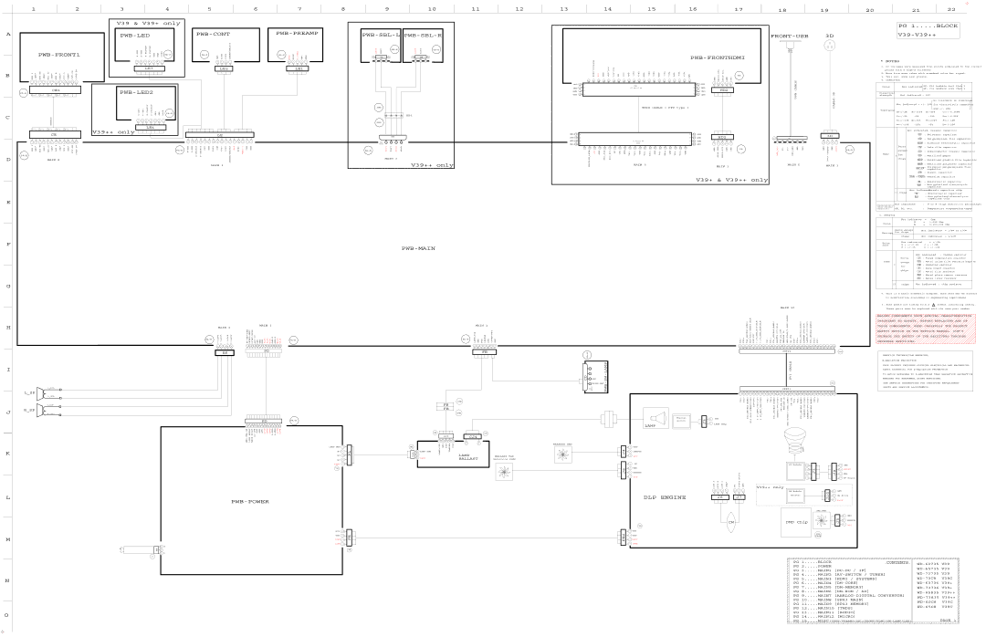
Mitsubishi Electronics WD-52527, WD-60C8, WD-65C8, WD-73C8 Gnd, Smp, Smr, Lamp GND, Cover-Det, Sensor, Dmdfan GND, DMD Temp

WD-60C8, WD-52527, WD-65C8, WD-73C8 specifications

The Mitsubishi Electronics WD-73C8, WD-73735, WD-73835, WD-73736, and WD-60735 are a series of high-performance DLP televisions known for their exceptional picture quality, advanced technology, and user-friendly features. These models, mainly targeting the large-screen home entertainment segment, are designed to deliver an immersive viewing experience.

One of the standout features of these televisions is their use of DLP (Digital Light Processing) technology, which ensures high brightness levels and vibrant colors. With Mitsubishi’s advanced DLP projection system, viewers can enjoy deeper blacks and a wide color gamut, making movies and sporting events come alive.

The WD-73C8 model, with its 73-inch screen, offers a colossal viewing area, making it an ideal choice for home theaters. Its Full HD resolution of 1920x1080 ensures that image clarity is never compromised, allowing viewers to see the finest details in high-definition content.

Similar in size, the WD-73735, WD-73835, and WD-73736 models also feature a 73-inch display, while the WD-60735 comes with a 60-inch screen. All models utilize Mitsubishi’s advanced Color Management System, which provides customizable color settings and enhances overall picture quality.

Another key technology integrated into these televisions is the Reality Creation feature, which enhances the sharpness and detail of standard-definition content. This means that older movies and TV shows can be upscaled to look more vibrant and clear, providing a better experience without the need for high-resolution sources.

The internal sound system of these models is engineered to complement their impressive visuals. Equipped with powerful speakers and advanced audio technologies, they deliver a cinematic sound experience that enhances everything from action scenes to quiet dialogue.

Connectivity options abound in these Mitsubishi TVs, with multiple HDMI ports, USB inputs, and even Ethernet connectivity for streaming services. This allows users to easily link their gaming consoles, Blu-ray players, and smart devices, further enhancing the versatility of the televisions.

Overall, the Mitsubishi Electronics WD-73C8, WD-73735, WD-73835, WD-73736, and WD-60735 models position themselves as excellent choices for consumers looking to elevate their home entertainment experience, combining cutting-edge technology with user-centric design. These televisions stand as a testament to Mitsubishi’s commitment to delivering high-quality, reliable products that enrich the viewing experience.