MS-7265 Mainboard
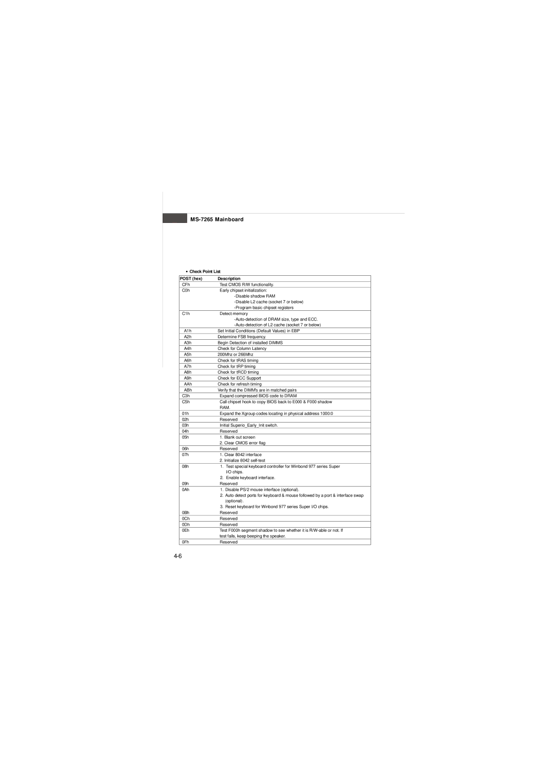
∙Check Point List
POST (hex) | Description | |
CFh | Test CMOS R/W functionality. | |
C0h | Early chipset initialization: | |
|
| |
|
| |
|
| |
C1h | Detect memory | |
|
| |
|
| |
A1h | Set Initial Conditions (Default Values) in EBP | |
A2h | Determine FSB frequency. | |
A3h | Begin Detection of installed DIMMS | |
A4h | Check for Column Latency | |
A5h | 200Mhz or 266Mhz | |
A6h | Check for tRAS timing | |
A7h | Check for tRP timing | |
A8h | Check for tRCD timing | |
A9h | Check for ECC Support | |
AAh | Check for refresh timing | |
ABh | Verify that the DIMM's are in matched pairs | |
C3h | Expand compressed BIOS code to DRAM | |
C5h | Call chipset hook to copy BIOS back to E000 & F000 shadow | |
| RAM. | |
01h | Expand the Xgroup codes locating in physical address 1000:0 | |
02h | Reserved | |
03h | Initial Superio_Early_Init switch. | |
04h | Reserved | |
05h | 1. Blank out screen | |
| 2. Clear CMOS error flag | |
06h | Reserved | |
07h | 1. Clear 8042 interface | |
| 2. Initialize 8042 | |
08h | 1. | Test special keyboard controller for Winbond 977 series Super |
|
| I/O chips. |
| 2. | Enable keyboard interface. |
09h | Reserved | |
0Ah | 1. Disable PS/2 mouse interface (optional). | |
| 2. Auto detect ports for keyboard & mouse followed by a port & interface swap | |
|
| (optional). |
| 3. Reset keyboard for Winbond 977 series Super I/O chips. | |
0Bh | Reserved | |
0Ch | Reserved | |
0Dh | Reserved | |
0Eh | Test F000h segment shadow to see whether it is | |
| test fails, keep beeping the speaker. | |
0Fh | Reserved | |