National Instruments user manual LM3647 Reference Design DEMO-BOARD

Models: LM3647

1 9
Download 9 pages 5.08 Kb
Page 8
Image 8

AN-1164

3.0 LM3647 REFERENCE DESIGN DEMO-BOARD

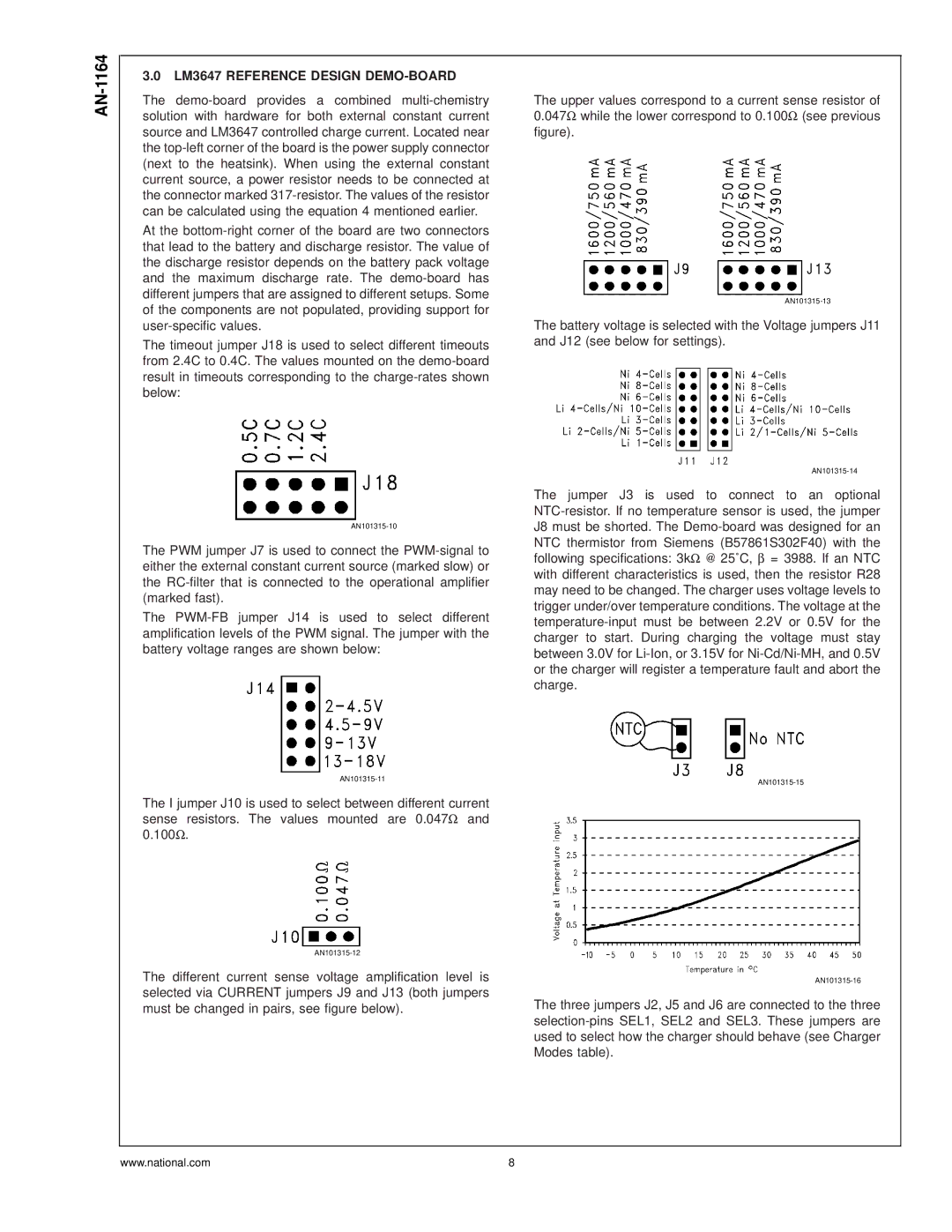
The demo-board provides a combined multi-chemistry solution with hardware for both external constant current source and LM3647 controlled charge current. Located near the top-left corner of the board is the power supply connector (next to the heatsink). When using the external constant current source, a power resistor needs to be connected at the connector marked 317-resistor. The values of the resistor can be calculated using the equation 4 mentioned earlier.

At the bottom-right corner of the board are two connectors that lead to the battery and discharge resistor. The value of the discharge resistor depends on the battery pack voltage and the maximum discharge rate. The demo-board has different jumpers that are assigned to different setups. Some of the components are not populated, providing support for user-specific values.

The timeout jumper J18 is used to select different timeouts from 2.4C to 0.4C. The values mounted on the demo-board result in timeouts corresponding to the charge-rates shown below:

AN101315-10

The PWM jumper J7 is used to connect the PWM-signal to either the external constant current source (marked slow) or the RC-filter that is connected to the operational amplifier (marked fast).

The PWM-FB jumper J14 is used to select different amplification levels of the PWM signal. The jumper with the battery voltage ranges are shown below:

AN101315-11

The I jumper J10 is used to select between different current sense resistors. The values mounted are 0.047Ω and 0.100Ω.

AN101315-12

The different current sense voltage amplification level is selected via CURRENT jumpers J9 and J13 (both jumpers must be changed in pairs, see figure below).

The upper values correspond to a current sense resistor of 0.047Ω while the lower correspond to 0.100Ω (see previous figure).

AN101315-13

The battery voltage is selected with the Voltage jumpers J11 and J12 (see below for settings).

AN101315-14

The jumper J3 is used to connect to an optional NTC-resistor. If no temperature sensor is used, the jumper J8 must be shorted. The Demo-board was designed for an NTC thermistor from Siemens (B57861S302F40) with the following specifications: 3kΩ @ 25ÊC, β = 3988. If an NTC with different characteristics is used, then the resistor R28 may need to be changed. The charger uses voltage levels to trigger under/over temperature conditions. The voltage at the temperature-input must be between 2.2V or 0.5V for the charger to start. During charging the voltage must stay between 3.0V for Li-Ion, or 3.15V for Ni-Cd/Ni-MH, and 0.5V or the charger will register a temperature fault and abort the charge.

AN101315-15

AN101315-16

The three jumpers J2, J5 and J6 are connected to the three selection-pins SEL1, SEL2 and SEL3. These jumpers are used to select how the charger should behave (see Charger Modes table).

www.national.com

8

Page 8
Image 8
National Instruments user manual LM3647 Reference Design DEMO-BOARD

LM3647 specifications

The National Instruments LM3647 is a versatile and advanced power management integrated circuit designed specifically for applications in mobile and portable devices. This device provides an efficient power supply solution that caters to the demands of today's sophisticated electronics.

One of the main features of the LM3647 is its ability to deliver a highly accurate output voltage. With a low output voltage ripple, it ensures that sensitive components receive stable power, thereby enhancing the performance and reliability of the system. The device typically uses a constant on-time control scheme, which allows for rapid transient response and improves overall efficiency, especially during dynamic load changes common in portable devices.

The LM3647 offers an impressive input voltage range, typically from 2.5V to 5.5V, making it compatible with a wide range of power sources, including lithium-ion batteries and USB power. Additionally, the device is highly efficient, boasting peak efficiencies of over 95%. This efficiency translates to extended battery life, a crucial factor for portable electronics.

Another significant characteristic of the LM3647 is its integrated power path management capability. This feature allows it to intelligently manage power distribution between the battery and the load, ensuring seamless transitions between battery and wall power, and providing system protection from overloads and short circuits.

The LM3647 also supports a flexible output configuration, featuring multiple outputs that can be independently programmed. This flexibility is particularly beneficial in applications such as smartphones, tablets, and wearables that require multiple voltage rails for various components, including processors, displays, and sensors.

Moreover, the LM3647 incorporates advanced thermal management techniques. With a package designed to dissipate heat efficiently, it helps maintain operational stability and longevity of the device even under heavy load conditions.

In summary, the National Instruments LM3647 stands out as a high-performance power management IC leveraging cutting-edge technologies to provide efficient power solutions for mobile and portable devices. Its features, including high efficiency, accurate output voltage, integrated power path management, and flexible output configurations, combined with robust thermal characteristics, make it an excellent choice for designers aiming for optimal power management in their electronic devices.