LC87F57C8A 
Overview
The LC87F57C8A is an
Functions
Timers
·One
·One
·Four
·Clock time base timer
![]()
(Can count a clock signal up to 20 MHz when a 10 MHz main clock frequency is used.)
 SIO
SIO
·Two
- Maximum clock: 4/3 tCYC
·One
- Asynchronous: 8 to 2048 tCYC, Synchronous: 2 to 512 tCYC |
|
|
|
|
| ||||
A/D converter: |
|
|
|
|
|
| |||
PWM: two |
| Block Diagram |
|
| |||||
Parallel interface (switchable polarity, can perform read and write |
|
|
|
|
| ||||
operations in 1·tCYC) |
|
|
|
|
|
|
| ||
Remote control receiver (using the P73/INT3/T0IN shared function pin) |
| Interrupt control | IR | PLA | |||||
Watchdog timer (Uses an external RC circuit) |
| ||||||||
|
|
|
|
| |||||
Interrupts |
|
|
|
|
| Standby control | Flash ROM | ||
· 20 interrupt sources with 10 vector locations (Multiple interrupts |
| CF | Clock generator |
|
| ||||
supported using three interrupt levels: low level (L), high level (H), |
|
|
| ||||||
| RC |
|
| ||||||
and maximum level (X)) |
|
|
| PC | |||||
|
| X'tal |
| ||||||
|
|
|
| ||||||
|
|
|
|
| |||||
· 16 bits | 8 bits | (Execution time: 5 tCYC) | SIO 0 |
| Bus |
| ACC | ||
· 24 bits | 16 bits (Execution time: 12 tCYC) |
|
| interface |
|
| |||
SIO 1 |
| Port 0 | Register B | ||||||
· 16 bits ⎟ 8 bits | (Execution time: 8 tCYC) |
| |||||||
|
|
|
|
| |||||
· 24 bits ⎟ 16 bits (Execution time: 12 tCYC) | SIO 2 |
| Port 1 | Register C | |||||
System clock divider function |
| Timer 0 |
| Port 3 |
| ALU | |||
Standby functions |
|
|
|
|
|
| |||
|
| Timer 1 |
| Port 7 |
|
| |||
· Halt mode: instruction execution stopped, peripheral circuit |
|
|
| ||||||
|
|
|
|
| |||||
operation continues |
|
| Timer 4 |
| Port 8 |
| PSW | ||
· Hold mode: instruction execution stopped, peripheral circuit | Timer 5 |
| ADC |
| RAR | ||||
operation stopped |
|
|
|
| |||||
|
|
|
| INT0 to INT3 |
|
| |||
· Crystal hold mode: instruction execution stopped, peripheral | PWM0 |
|
| RAM | |||||
|
| noise rejection |
|
| |||||
circuit operation stopped except for the clock time base timer | PWM1 |
| Port 2 | Stack pointer | |||||
Package: QIP64E (14 | 14), SQFP64 (10 | 10) |
|
| INT4,5 |
|
| ||
Clock time base |
| Watchdog | |||||||
|
|
|
|
| Parallel | ||||
|
|
|
|
| timer | ||||
|
|
|
|
| timer |
| |||
|
|
|
|
|
| interface |
|
| |
|
|
|
|
|
|
|
|
| |
|
|
|
|
| Timer 6 |
| Port A |
|
|
|
|
|
|
|
|
| Port B |
|
|
|
|
|
|
| Timer 7 |
| Port C |
|
|
|
|
|
|
|
|
|
|
| |
This flash memory product is manufactured and sold by SANYO Electric Co., Ltd. under license from Silicon Storage Technologies, Inc. (SST).
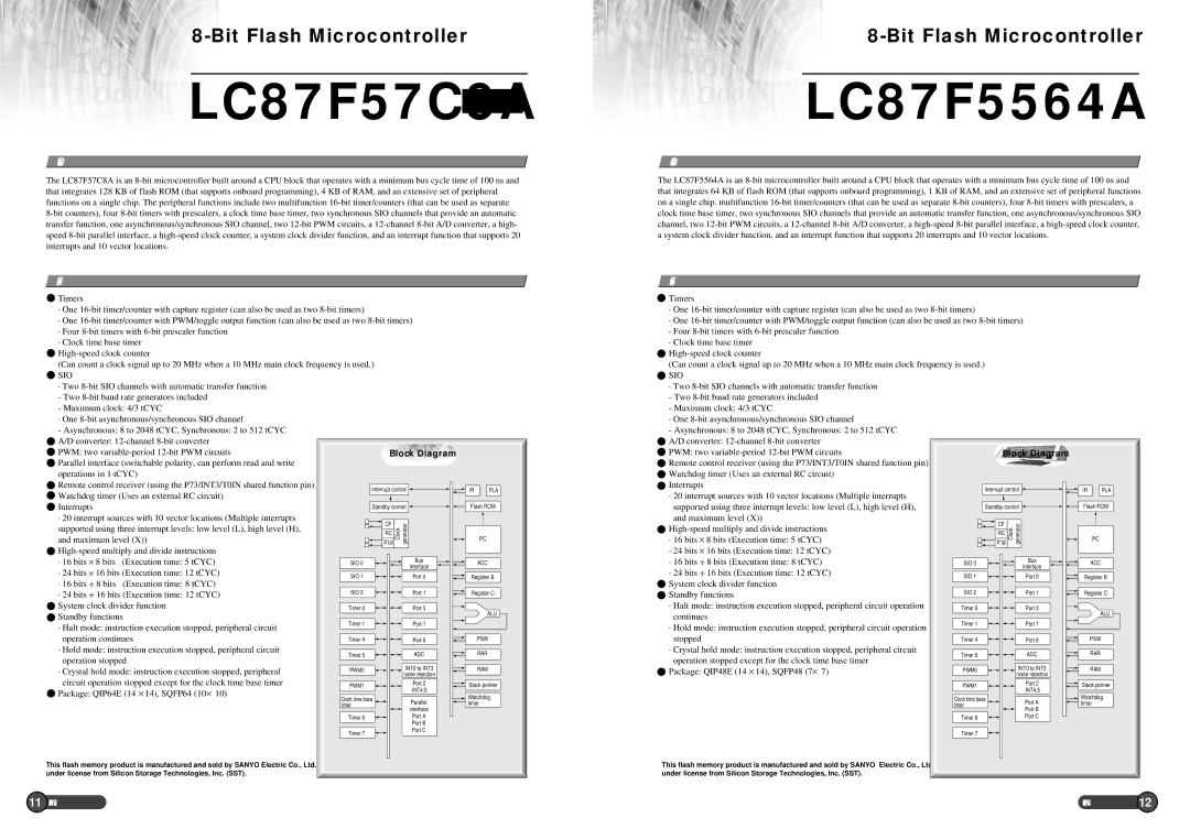
LC87F5564A
Overview
The LC87F5564A is an
Functions
Timers
·One
·One
·Four
·Clock time base timer
![]()
(Can count a clock signal up to 20 MHz when a 10 MHz main clock frequency is used.)
![]() SIO
SIO
·Two
- Maximum clock: 4/3 tCYC
·One
- Asynchronous: 8 to 2048 tCYC, Synchronous: 2 to 512 tCYC |
|
|
|
|
| |||
A/D converter: |
|
|
|
|
|
| ||
PWM: two |
| Block Diagram |
|
| ||||
Remote control receiver (using the P73/INT3/T0IN shared function pin) |
|
|
|
|
| |||
Watchdog timer (Uses an external RC circuit) |
|
|
|
|
| |||
Interrupts |
|
|
|
| Interrupt control | IR | PLA | |
· 20 interrupt sources with 10 vector locations (Multiple interrupts |
| |||||||
|
|
|
|
| ||||
supported using three interrupt levels: low level (L), high level (H), |
| Standby control | Flash ROM | |||||
and maximum level (X)) |
|
| CF | Clock generator |
|
| ||
|
|
| ||||||
| RC |
|
| |||||
· 16 bits | 8 bits (Execution time: 5 tCYC) |
|
| PC | ||||
| X'tal |
| ||||||
|
|
| ||||||
· 24 bits | 16 bits (Execution time: 12 tCYC) |
|
|
|
|
| ||
· 16 bits ⎟ 8 bits (Execution time: 8 tCYC) | SIO 0 |
| Bus |
| ACC | |||
· 24 bits ⎟ 16 bits (Execution time: 12 tCYC) |
|
| interface |
|
| |||
SIO 1 |
| Port 0 | Register B | |||||
System clock divider function |
|
| ||||||
| SIO 2 |
|
|
|
| |||
Standby functions |
|
|
| Port 1 | Register C | |||
· Halt mode: instruction execution stopped, peripheral circuit operation | Timer 0 |
| Port 3 |
| ALU | |||
continues |
|
|
|
|
|
| ||
|
| Timer 1 |
| Port 7 |
|
| ||
· Hold mode: instruction execution stopped, peripheral circuit operation |
|
|
| |||||
|
|
|
|
| ||||
stopped |
|
|
| Timer 4 |
| Port 8 |
| PSW |
· Crystal hold mode: instruction execution stopped, peripheral circuit | Timer 5 |
| ADC |
| RAR | |||
operation stopped except for the clock time base timer |
|
| ||||||
|
| INT0 to INT3 |
|
| ||||
Package: QIP48E (14 | 14), SQFP48 (7 | 7) | PWM0 |
|
| RAM | ||
|
| noise rejection |
|
| ||||
|
|
|
| PWM1 |
| Port 2 | Stack pointer | |
|
|
|
|
| INT4,5 | |||
|
|
|
|
|
|
|
| |
|
|
|
| Clock time base | Port A | Watchdog | ||
|
|
|
| timer | ||||
|
|
|
| timer |
| |||
|
|
|
|
| Port B |
|
| |
|
|
|
|
|
|
|
| |
|
|
|
| Timer 6 |
| Port C |
|
|
This flash memory product is manufactured and sold by SANYO Electric Co., Ltd. under license from Silicon Storage Technologies, Inc. (SST).
11 SANYO TV . VCR | SANYO TV . VCR 12 |