ST973402SS, ST9146802SS specifications
The Seagate ST973402SS and ST9146802SS are high-performance, enterprise-grade hard drives designed to meet the demanding needs of data-intensive applications. These drives are part of Seagate's Savvio and Barracuda product lines, aimed specifically at businesses and institutions requiring reliability, speed, and efficiency in storage solutions.The ST973402SS is a 73GB, 2.5-inch hard drive, while the ST9146802SS offers a larger capacity of 146GB. Both models utilize a 10,000 RPM spindle speed, which significantly enhances their ability to handle fast data read and write operations. This speed ensures reduced latency and improved overall performance, making them ideal for environments where rapid access to data is crucial.
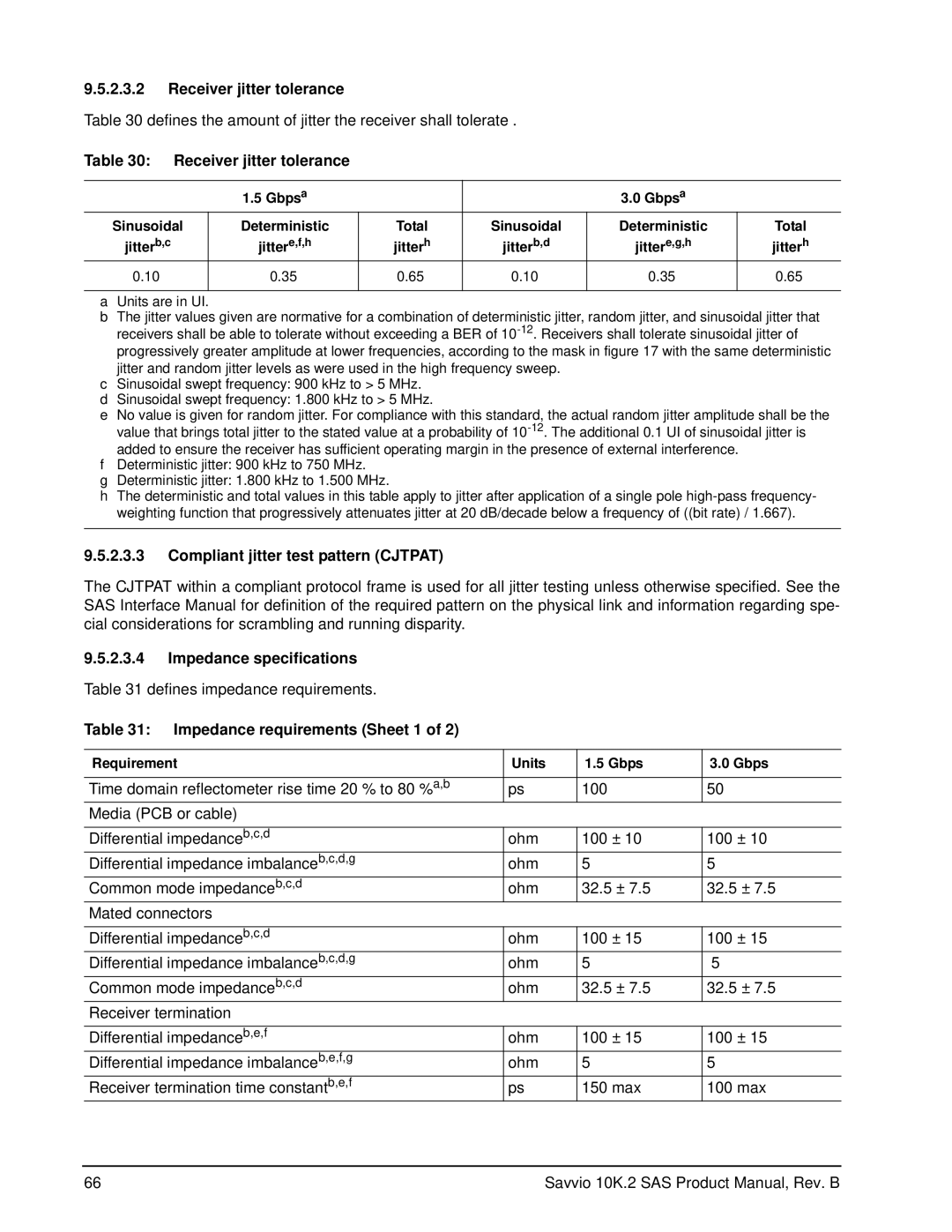
One of the standout features of these drives is their support for Serial Attached SCSI (SAS) interface. SAS technology provides a point-to-point connection, which allows for increased data transfer rates compared to traditional SATA drives. The ST973402SS and ST9146802SS are capable of transferring data at speeds of up to 600 MB/s, facilitating efficient data transfers in enterprise systems.
In terms of reliability, both models offer advanced features designed to improve data integrity and durability. They are built to withstand high workloads, with an annualized workload rate of up to 550 TB per year. This makes them well-suited for applications like databases and transactional storage, where sustained performance is required. Additionally, the drives feature Seagate’s PowerFit technology, which optimizes performance while minimizing power consumption.
To enhance data security, the drives come equipped with self-encrypting technology, ensuring that sensitive data is protected through hardware-based encryption. This is particularly important in environments where data breaches can lead to significant operational impacts.
The drives are also designed to operate efficiently in terms of thermal management, featuring robust heat dissipation capabilities. This helps to maintain optimal performance levels while prolonging the lifespan of the drives.
Overall, the Seagate ST973402SS and ST9146802SS are robust and reliable hard drives that cater to the needs of enterprise environments, combining high capacity, exceptional speed, advanced security features, and energy efficiency to help businesses maintain and manage large volumes of data effectively. With their proven performance and innovative technologies, these drives are well-equipped to support a wide range of applications in modern data centers.