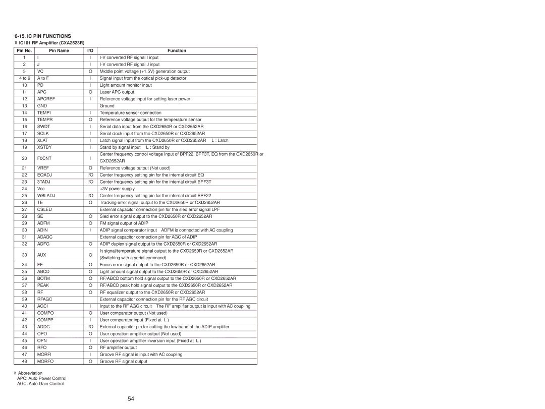
MDS-JD320 specifications
The Sony MDS-JD320 is a MiniDisc recorder that exemplifies the cutting-edge technology of the late 1990s and early 2000s. Designed for both amateur and professional audiophiles, it delivers superior sound quality and an array of features that enhance user experience and functionality. Key to its appeal is its remarkable sound reproduction capabilities, which are achieved through Sony's proprietary technologies, including the ATRAC (Adaptive Transform Acoustic Coding) compression format. This format allows for efficient audio storage without sacrificing sound fidelity, ensuring that each recording is as rich and dynamic as the original source.One of the standout features of the MDS-JD320 is its ability to create, edit, and playback CDs and MiniDiscs with remarkable ease. Thanks to its digital optical input and output, users can connect the device to various audio sources, such as CD players or mixing boards, to make high-quality recordings. The device supports various recording modes, including long play, which enables users to extend their recording time without significant compromise on audio quality.
The MDS-JD320 also boasts a user-friendly interface, which includes an LCD display that conveniently shows essential information such as track numbers, remaining time, and recording mode. Furthermore, an intuitive remote control offers added convenience, allowing users to navigate through their music collections without having to physically interact with the device.
In terms of connectivity, the MDS-JD320 features not only digital inputs and outputs but also analog connections, making it versatile for various setups. Additionally, the device includes extensive editing features, such as track splitting, combining, and renaming, empowering users to customize their recordings easily.
Moreover, the MDS-JD320's compact design fits seamlessly into any audio setup, making it an attractive choice for both home recording enthusiasts and professionals. Its durable build quality ensures longevity, while its performance continues to impress even in today's digital audio landscape.
With its powerful combination of advanced technologies, ease of use, and high-quality audio performance, the Sony MDS-JD320 remains a sought-after component for collectors and audiophiles alike, representing an enduring legacy in the field of portable digital media solutions.
