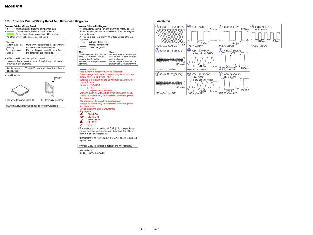
MZ-NF610 specifications
The Sony MZ-NF610 is a standout portable mini disc player and recorder that epitomizes the innovation synonymous with Sony in the early 2000s. Released as part of the Net MiniDisc series, it offered a convenient way to manage and enjoy music on the go. While the popularity of digital downloads and streaming services has eclipsed physical media formats, the MZ-NF610 remains a nostalgic piece of technology that reflects a unique era in personal audio.One of the main features of the MZ-NF610 is its large storage capacity, leveraging the MiniDisc format to offer up to 1GB of data storage on each disc. This allows music enthusiasts to store multiple albums or hours of music in a compact form. The device supports LP2 and LP4 recording modes, which not only provide flexibility in recording quality but also enhance the total recording time, making it ideal for long journeys or extensive music libraries.
The MZ-NF610 showcases SONY’s exceptional ATRAC3 encoding technology, which compresses audio files while preserving sound quality. This technology enables users to transfer music from CD directly to MiniDisc with impressive fidelity. Additionally, with its USB connection, the MZ-NF610 provides a seamless way to transfer music files from a computer, further enhancing its usability.
An important characteristic of the MZ-NF610 is its design. This model is compact, lightweight, and equipped with an easy-to-use interface, making it perfect for portability. The ergonomically designed controls simplify navigation through tracks and menus, while the backlit LCD display ensures visibility in various lighting conditions.
Battery life is another notable feature of the MZ-NF610, with the ability to run for long periods on a single charge. The player is powered by a rechargeable lithium-ion battery, which enhances its eco-friendliness and eliminates the need for disposable batteries.
Overall, the Sony MZ-NF610 is a remarkable combination of portability, audio quality, and user convenience. It highlights Sony’s commitment to pushing the boundaries of personal audio technology, making it a cherished collector's item for those who appreciate the charm of MiniDisc players. Even in an age dominated by digital streaming, the MZ-NF610 stands as a testament to the enduring appeal of physical media and the nostalgic experience it provides.

