THIS NOTE IS COMMON FOR PRINTED WIRING BOARDS AND SCHEMATIC DIAGRAMS.
• Waveform
1
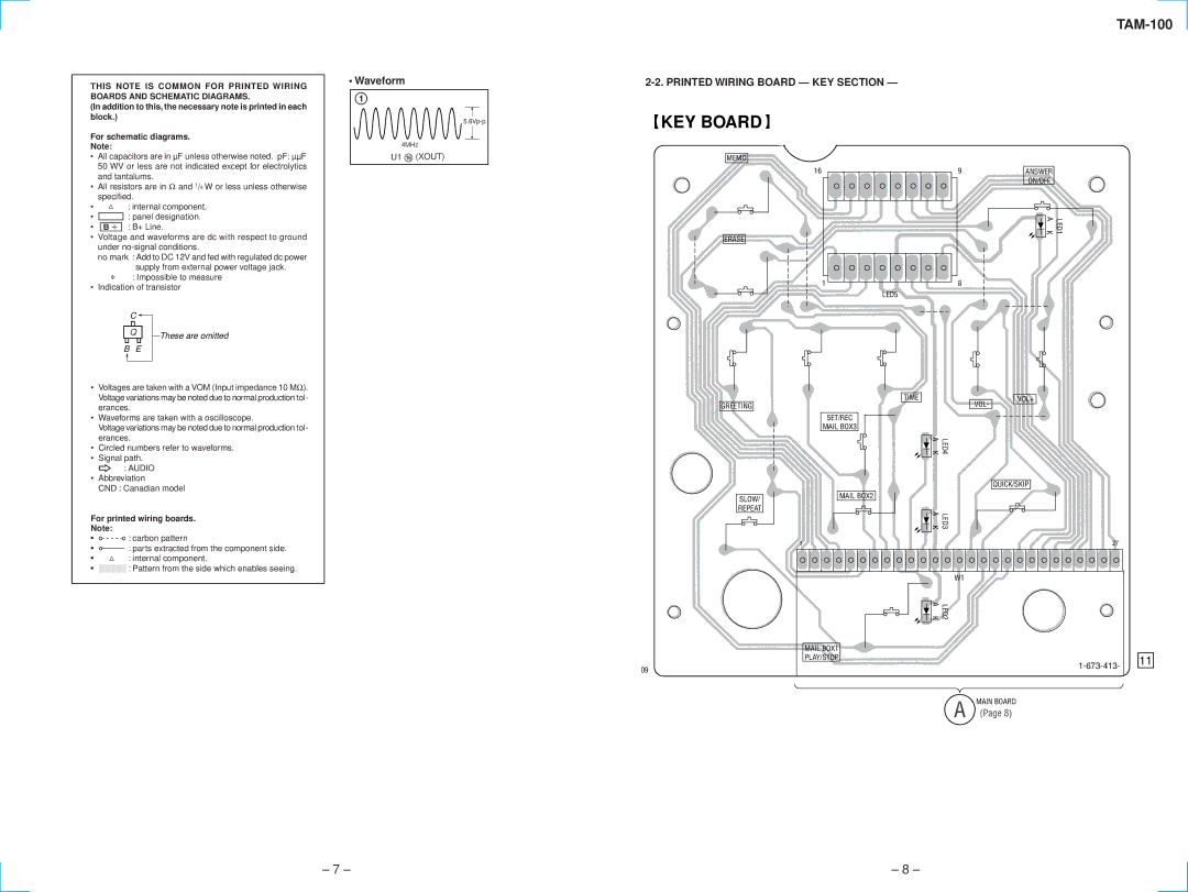
2-2. PRINTED WIRING BOARD — KEY SECTION —
(In addition to this, the necessary note is printed in each block.)
For schematic diagrams.
Note:
•All capacitors are in µF unless otherwise noted. pF: µµF 50 WV or less are not indicated except for electrolytics and tantalums.
•All resistors are in Ω and 1/4 W or less unless otherwise specified.
•¢ : internal component.
•C : panel designation.
•U : B+ Line.
•Voltage and waveforms are dc with respect to ground under
no mark : Add to DC 12V and fed with regulated dc power supply from external power voltage jack.
∗: Impossible to measure
•Indication of transistor
C |
|
Q | These are omitted |
|
BE
•Voltages are taken with a VOM (Input impedance 10 MΩ). Voltage variations may be noted due to normal production tol- erances.
•Waveforms are taken with a oscilloscope.
Voltage variations may be noted due to normal production tol- erances.
•Circled numbers refer to waveforms.
•Signal path.
F : AUDIO
•Abbreviation
CND : Canadian model
For printed wiring boards.
Note:
•![]()
![]() : carbon pattern
: carbon pattern
•X : parts extracted from the component side.
•¢ : internal component.
•b: Pattern from the side which enables seeing.
4MHz
U1 !§ (XOUT)
 KEY BOARD
MEMO
ERASE
GREETING
SLOW/
REPEAT
09
16 | 9 |
1 | 8 |
LED5
TIME
SET/REC
MAIL BOX3
LED4
A K
VOL-
ANSWER
ON/OFF
LED1
A K
VOL+
| QUICK/SKIP |
| MAIL BOX2 |
| LED3 A K |
1 | 27 |
| W1 |
| LED2 A K |
MAIL BOX1
PLAY/STOP
11
A | MAIN BOARD |
(Page 8) |
– 7 – | – 8 – |