CDX-CA850/CA850X/CA860X
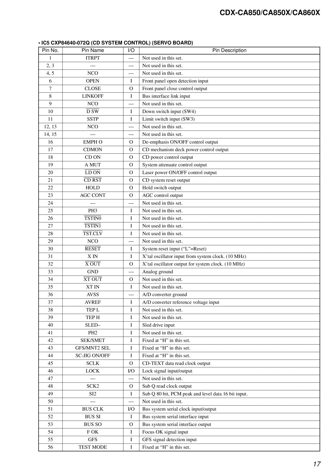
• IC5 CXP84640-072Q (CD SYSTEM CONTROL) (SERVO BOARD)
Pin No. | Pin Name | I/O | Pin Description | ||||||||||||
|
|
|
|
|
|
|
|
|
|
|
|
|
|
|
|
1 |
|
|
| ITRPT | — | Not used in this set. | |||||||||
|
|
|
|
|
|
|
|
|
|
|
|
|
|
|
|
2, 3 |
|
|
|
| — | — | Not used in this set. | ||||||||
|
|
|
|
|
|
|
|
|
|
|
|
|
|
|
|
4, 5 |
|
|
|
| NCO | — | Not used in this set. | ||||||||
|
|
|
|
|
|
|
|
|
|
|
|
|
|
|
|
6 |
|
|
| OPEN | I | Front panel open detection input | |||||||||
|
|
|
|
|
|
|
|
|
|
|
|
|
|
|
|
7 |
|
|
| CLOSE | O | Front panel close control output | |||||||||
|
|
|
|
|
|
|
|
|
|
|
|
|
|
|
|
8 | LINKOFF | I | Bus interface link input | ||||||||||||
|
|
|
|
|
|
|
|
|
|
|
|
|
|
|
|
9 |
|
|
|
| NCO | — | Not used in this set. | ||||||||
|
|
|
|
|
|
|
|
|
|
|
|
|
|
|
|
10 |
|
|
|
|
|
|
|
|
|
|
|
|
| I | Down switch input (SW4) |
|
|
|
| D SW | |||||||||||
|
|
|
|
|
|
|
|
|
|
|
|
|
|
|
|
11 |
|
|
|
| SSTP | I | Limit switch input (SW3) | ||||||||
|
|
|
|
|
|
|
|
|
|
|
|
|
|
|
|
12, 13 |
|
|
|
| NCO | — | Not used in this set. | ||||||||
|
|
|
|
|
|
|
|
|
|
|
|
|
|
|
|
14, 15 |
|
|
|
| — | — | Not used in this set. | ||||||||
|
|
|
|
|
|
|
|
|
|
|
|
|
|
|
|
16 |
| EMPH O | O | ||||||||||||
|
|
|
|
|
|
|
|
|
|
|
|
|
|
|
|
17 |
| CDMON | O | CD mechanism deck power control output | |||||||||||
|
|
|
|
|
|
|
|
|
|
|
|
|
|
|
|
18 |
|
|
| CD ON | O | CD power control output | |||||||||
|
|
|
|
|
|
|
|
|
|
|
|
|
|
|
|
19 |
|
|
| A MUT | O | System attenuate control output | |||||||||
|
|
|
|
|
|
|
|
|
|
|
|
|
|
|
|
20 |
|
|
|
|
|
|
|
|
|
|
| O | Laser power ON/OFF control output | ||
|
|
| LD ON | ||||||||||||
|
|
|
|
|
|
|
|
|
|
|
|
|
|
|
|
21 |
|
|
|
|
|
|
|
|
|
| O | CD system reset output | |||
|
| CD RST | |||||||||||||
|
|
|
|
|
|
|
|
|
|
|
|
|
|
|
|
22 |
|
|
| HOLD | O | Hold switch output | |||||||||
|
|
|
|
|
|
|
|
|
|
|
|
|
|
|
|
23 | AGC CONT | O | AGC control output | ||||||||||||
|
|
|
|
|
|
|
|
|
|
|
|
|
|
|
|
24 |
|
|
|
| — | — | Not used in this set. | ||||||||
|
|
|
|
|
|
|
|
|
|
|
|
|
|
|
|
25 |
|
|
|
| PH3 | I | Not used in this set. | ||||||||
|
|
|
|
|
|
|
|
|
|
|
|
|
|
|
|
26 |
|
|
|
|
|
|
|
|
| I | Not used in this set. | ||||
|
| TSTIN0 | |||||||||||||
|
|
|
|
|
|
|
|
|
|
|
|
|
|
|
|
27 |
|
|
|
|
|
|
|
| I | Not used in this set. | |||||
|
| TSTIN1 | |||||||||||||
|
|
|
|
|
|
|
|
|
|
|
|
|
|
|
|
28 |
|
|
|
|
|
|
| I | Not used in this set. | ||||||
| TST.CLV | ||||||||||||||
|
|
|
|
|
|
|
|
|
|
|
|
|
|
|
|
29 |
|
|
|
| NCO | — | Not used in this set. | ||||||||
|
|
|
|
|
|
|
|
|
|
|
|
|
|
|
|
30 |
|
|
|
|
|
|
| I | System reset input (“L”=Reset) | ||||||
|
|
| RESET | ||||||||||||
|
|
|
|
|
|
|
|
|
|
|
|
|
|
|
|
31 |
|
|
|
| X IN | I | X’tal oscillator input from system clock. (10 MHz) | ||||||||
|
|
|
|
|
|
|
|
|
|
|
|
|
|
|
|
32 |
|
|
|
|
|
| O | X’tal oscillator output for system clock. (10 MHz) | |||||||
|
|
| X OUT | ||||||||||||
|
|
|
|
|
|
|
|
|
|
|
|
|
|
|
|
33 |
|
|
|
| GND | — | Analog ground | ||||||||
|
|
|
|
|
|
|
|
|
|
|
|
|
|
|
|
34 |
|
|
|
| O | Not used in this set. | |||||||||
|
| XT OUT | |||||||||||||
|
|
|
|
|
|
|
|
|
|
|
|
|
|
|
|
35 |
|
|
| XT IN | I | Not used in this set. | |||||||||
|
|
|
|
|
|
|
|
|
|
|
|
|
|
|
|
36 |
|
|
|
| AVSS | — | A/D converter ground | ||||||||
|
|
|
|
|
|
|
|
|
|
|
|
|
|
|
|
37 |
|
|
| AVREF | I | A/D converter reference voltage input | |||||||||
|
|
|
|
|
|
|
|
|
|
|
|
|
|
|
|
38 |
|
|
| TEP L | I | Not used in this set. | |||||||||
|
|
|
|
|
|
|
|
|
|
|
|
|
|
|
|
39 |
|
|
| TEP H | I | Not used in this set. | |||||||||
|
|
|
|
|
|
|
|
|
|
|
|
|
|
|
|
40 |
|
|
| SLED– | I | Sled drive input | |||||||||
|
|
|
|
|
|
|
|
|
|
|
|
|
|
|
|
41 |
|
|
|
| PH2 | I | Not used in this set. | ||||||||
|
|
|
|
|
|
|
|
|
|
|
|
|
|
|
|
42 | SEK/SMET | I | Fixed at “H” in this set. | ||||||||||||
|
|
|
|
|
|
|
|
|
|
|
|
|
|
|
|
43 | GFS/MNT2 SEL | I | Fixed at “H” in this set. | ||||||||||||
|
|
|
|
|
|
|
|
|
|
|
|
|
|
|
|
44 | I | Fixed at “H” in this set. | |||||||||||||
|
|
|
|
|
|
|
|
|
|
|
|
|
|
|
|
45 |
|
|
|
| SCLK | O | |||||||||
|
|
|
|
|
|
|
|
|
|
|
|
|
|
|
|
46 |
|
|
| LOCK | I/O | Lock signal input/output | |||||||||
|
|
|
|
|
|
|
|
|
|
|
|
|
|
|
|
47 |
|
|
|
| — | — | Not used in this set. | ||||||||
|
|
|
|
|
|
|
|
|
|
|
|
|
|
|
|
48 |
|
|
|
| SCK2 | O | Sub Q read clock output | ||||||||
|
|
|
|
|
|
|
|
|
|
|
|
|
|
|
|
49 |
|
|
|
| SI2 | I | Sub Q 80 bit, PCM peak and level data 16 bit input. | ||||||||
|
|
|
|
|
|
|
|
|
|
|
|
|
|
|
|
50 |
|
|
|
| — | — | Not used in this set. | ||||||||
|
|
|
|
|
|
|
|
|
|
|
|
|
|
|
|
51 | BUS CLK | I/O | Bus system serial clock input/output | ||||||||||||
|
|
|
|
|
|
|
|
|
|
|
|
|
|
|
|
52 |
|
|
| BUS SI | I | Bus system serial interface input | |||||||||
|
|
|
|
|
|
|
|
|
|
|
|
|
|
|
|
53 |
|
| BUS SO | O | Bus system serial interface output | ||||||||||
|
|
|
|
|
|
|
|
|
|
|
|
|
|
|
|
54 |
|
|
|
| F OK | I | Focus OK signal input | ||||||||
|
|
|
|
|
|
|
|
|
|
|
|
|
|
|
|
55 |
|
|
|
| GFS | I | GFS signal detection input | ||||||||
|
|
|
|
|
|
|
|
|
|
|
|
|
|
|
|
56 | TEST MODE | I | Fixed at “H” in this set. | ||||||||||||
|
|
|
|
|
|
|
|
|
|
|
|
|
|
|
|
17