(1/2)
Varistors(SMD)
For High-speed Differential Signal Line
AVF16 Series
Conformity to RoHS Directive
A
FEATURES
•Chip size: 1608 (L1.6⋅ W0.8mm), applicable in 2
•2GHz or more of cutoff frequency in differential mode (Sdd21).
•Superior electrostatic absorption characteristics due to reduction of varistor voltage.
•Meeting Electrostatic Discharge Test
APPLICATIONS
•Protective circuit for
•HDMI, USB, IEEE1394, etc.
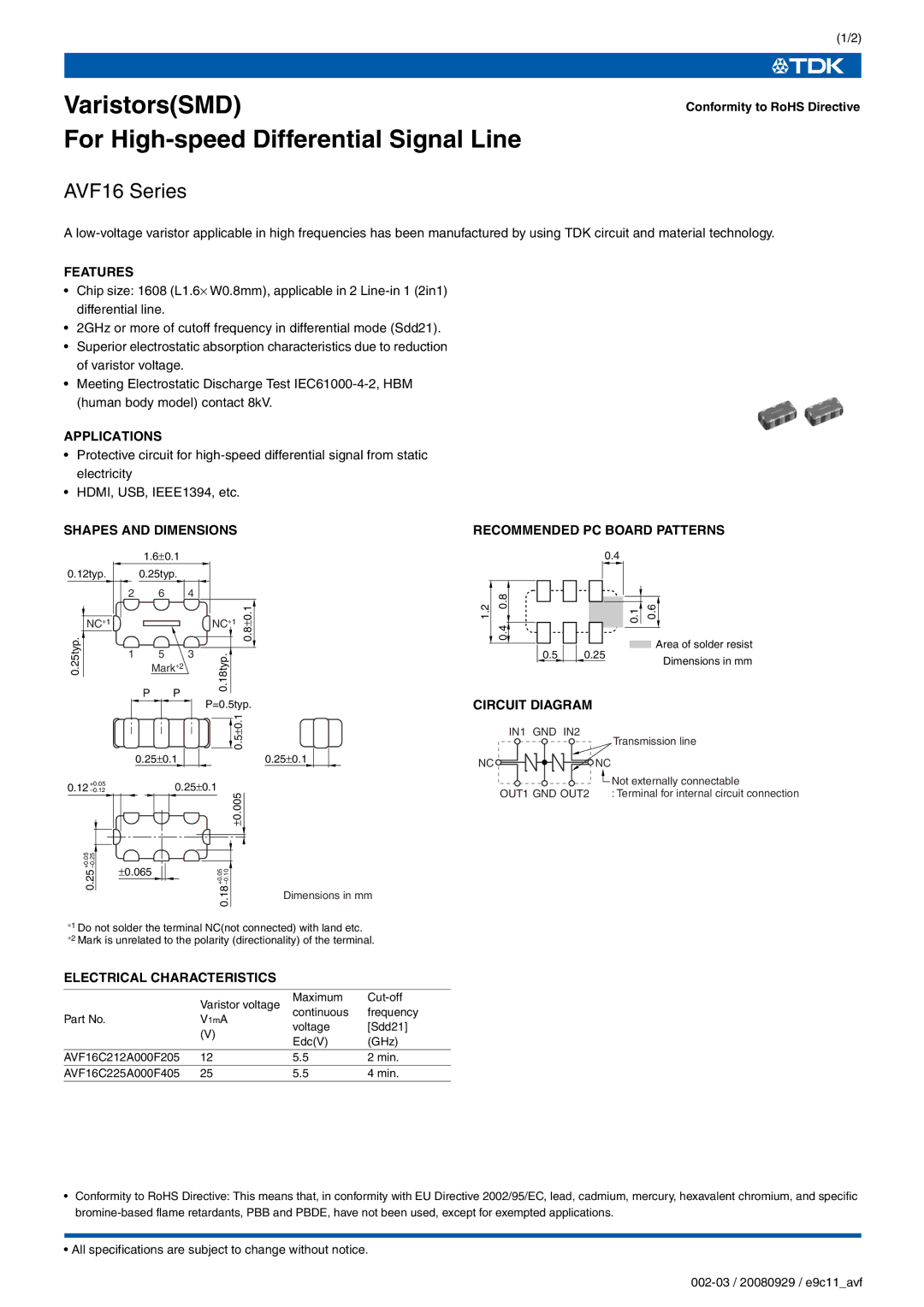
SHAPES AND DIMENSIONS
|
| 1.6±0.1 |
|
|
| |
0.12typ. |
| 0.25typ. |
|
|
| |
| 2 |
| 6 | 4 |
|
|
NC∗1 |
|
|
|
| NC∗1 | ±0.1 |
0.25typ. | 1 |
| 5 | 3 | 0.18typ. | 0.8 |
|
|
|
| |||
|
|
| Mark∗2 |
|
|
|
|
| P | P |
| P=0.5typ. | |
|
|
|
|
| ||
|
|
|
|
| 0.5±0.1 | |
|
| 0.25±0.1 |
|
| 0.25±0.1 | |
RECOMMENDED PC BOARD PATTERNS
|
|
|
|
|
|
| 0.4 |
|
|
|
|
|
| |||||
|
|
|
|
|
|
|
|
|
|
|
|
|
|
|
|
|
|
|
|
| 0.8 |
|
|
|
|
|
|
|
|
|
|
|
|
|
|
|
|
1.2 |
|
|
|
|
|
|
|
|
|
|
| 0.1 |
| 0.6 |
| |||
|
| 0.4 |
|
|
|
|
|
|
|
|
|
|
|
|
|
| Area of solder resist | |
|
|
|
|
|
|
|
|
|
|
|
|
|
|
|
|
| ||
|
|
|
|
| 0.5 |
| 0.25 |
|
|
|
|
|
|
| Dimensions in mm | |||
|
|
|
|
|
|
|
|
|
|
|
|
|
|
|
|
|
| |
CIRCUIT DIAGRAM
IN1 GND IN2
Transmission line
NC ![]()
![]()
![]()
![]()
![]()
![]() NC
NC
0.12
+0.05 |
|
|
|
|
|
| |
| |||
0.25 |
|
| |
±0.065
0.25±0.1
±0.005
+0.05 |
| |
0.18 | Dimensions in mm | |
|
| |
| Not externally connectable |
OUT1 GND OUT2 | : Terminal for internal circuit connection |
∗1 Do not solder the terminal NC(not connected) with land etc.
∗2 Mark is unrelated to the polarity (directionality) of the terminal.
ELECTRICAL CHARACTERISTICS
| Varistor voltage | Maximum | ||
| continuous | frequency | ||
Part No. | V1mA | |||
voltage | [Sdd21] | |||
| (V) | |||
| Edc(V) | (GHz) | ||
|
| |||
AVF16C212A000F205 | 12 | 5.5 | 2 min. | |
AVF16C225A000F405 | 25 | 5.5 | 4 min. |
•Conformity to RoHS Directive: This means that, in conformity with EU Directive 2002/95/EC, lead, cadmium, mercury, hexavalent chromium, and specific
•All specifications are subject to change without notice.
