www.ti.com

Circuit Description

3 Circuit Description

3.1Schematic Diagram

The schematic diagram for the EVM is in Section 5.3 of this document.

3.2Circuit Function

The following paragraphs describe the function of individual circuits. See the data sheet for complete device operating characteristics.

3.2.1Configuration Options

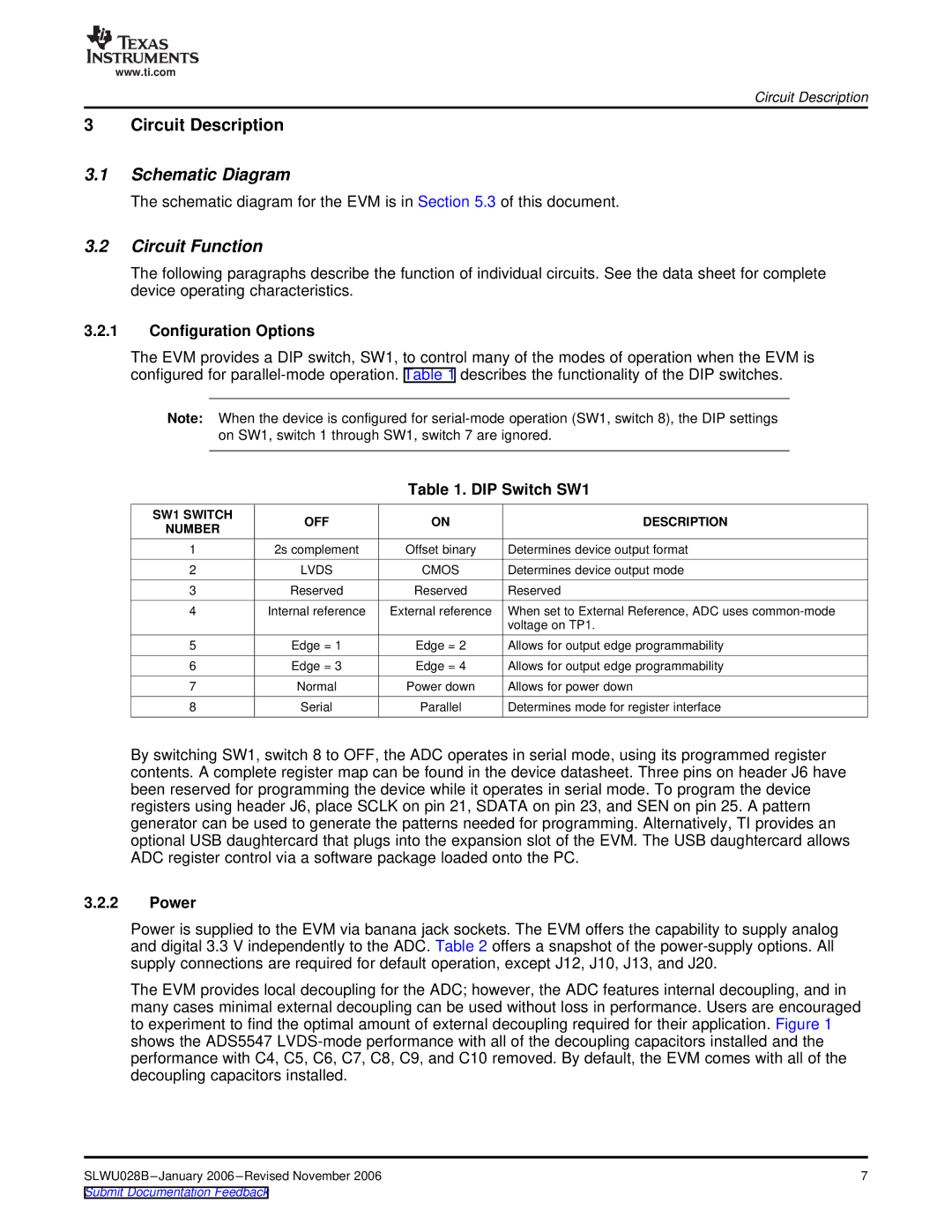
The EVM provides a DIP switch, SW1, to control many of the modes of operation when the EVM is configured for parallel-mode operation. Table 1 describes the functionality of the DIP switches.

Note: When the device is configured for serial-mode operation (SW1, switch 8), the DIP settings on SW1, switch 1 through SW1, switch 7 are ignored.

Table 1. DIP Switch SW1

SW1 SWITCH

OFF

ON

DESCRIPTION

NUMBER


1

2s complement

Offset binary

Determines device output format

2

LVDS

CMOS

Determines device output mode

3

Reserved

Reserved

Reserved

4

Internal reference

External reference

When set to External Reference, ADC uses common-mode


voltage on TP1.

5

Edge = 1

Edge = 2

Allows for output edge programmability

6

Edge = 3

Edge = 4

Allows for output edge programmability

7

Normal

Power down

Allows for power down

8

Serial

Parallel

Determines mode for register interface

By switching SW1, switch 8 to OFF, the ADC operates in serial mode, using its programmed register contents. A complete register map can be found in the device datasheet. Three pins on header J6 have been reserved for programming the device while it operates in serial mode. To program the device registers using header J6, place SCLK on pin 21, SDATA on pin 23, and SEN on pin 25. A pattern generator can be used to generate the patterns needed for programming. Alternatively, TI provides an optional USB daughtercard that plugs into the expansion slot of the EVM. The USB daughtercard allows ADC register control via a software package loaded onto the PC.

3.2.2Power

Power is supplied to the EVM via banana jack sockets. The EVM offers the capability to supply analog and digital 3.3 V independently to the ADC. Table 2 offers a snapshot of the power-supply options. All supply connections are required for default operation, except J12, J10, J13, and J20.

The EVM provides local decoupling for the ADC; however, the ADC features internal decoupling, and in many cases minimal external decoupling can be used without loss in performance. Users are encouraged to experiment to find the optimal amount of external decoupling required for their application. Figure 1 shows the ADS5547 LVDS-mode performance with all of the decoupling capacitors installed and the performance with C4, C5, C6, C7, C8, C9, and C10 removed. By default, the EVM comes with all of the decoupling capacitors installed.

SLWU028B –January 2006 –Revised November 2006

7

Submit Documentation Feedback

Page 7
Image 7
Texas Instruments 45, 46, 27, 47, ADS5525 Schematic Diagram, Circuit Function, Configuration Options, DIP Switch SW1, Power

ADS5525, 27, 47, 45, 46 specifications

Texas Instruments is a leader in the field of analog and mixed-signal semiconductors and offers a diverse portfolio of high-performance products. Among its notable offerings are the ADCs (Analog-to-Digital Converters) such as the TI 46, 45, 47, 27, and the ADS5525. These devices are engineered to meet the demanding requirements of various applications, including communications, industrial, and medical systems.

The Texas Instruments 46 series ADCs are recognized for their high speed and precision. They utilize a 14-bit architecture with sampling rates of up to 1.5 GSPS, which makes them ideal for high-frequency applications such as communications and instrumentation. One of the key features is their ability to support a wide input bandwidth, which allows for accurate conversions of high-frequency signals.

The 45 series, similar in architecture, excels in environments where power efficiency is paramount. These ADCs are designed to consume less power while maintaining high performance. They offer a flexible sampling rate, providing options for both lower and higher intensity applications. This versatility is essential for handheld and portable devices where battery life is crucial.

Moving on to the 47 family, these devices focus on achieving high dynamic range and low distortion. Their architecture includes sophisticated digital filter options, enhancing the capability of noise reduction and signal integrity. With an impressive signal-to-noise ratio, the 47 series finds its usage in systems where performance cannot be compromised, such as high-end audio and video applications.

The 27 series ADCs provide an excellent combination of high performance and low latency, making them suitable for real-time analysis in various scenarios. They are equipped with advanced data acquisition features and can communicate seamlessly with modern digital signal processors and microcontrollers.

Finally, the ADS5525 is a standout in the lineup, offering a 12-bit resolution at a maximum sampling rate of 125 MSPS. This device is designed for a range of applications, including medical imaging and ultrasound systems. It boasts features such as an integrated digital filter and multiple power-saving modes, making it versatile and efficient in terms of energy consumption.

In summary, Texas Instruments' ADC lineup, including the 46, 45, 47, 27, and ADS5525, offers numerous features and technologies, catering to a wide range of applications through their respective specifications of speed, power efficiency, dynamic range, and ease of integration. These devices illustrate Texas Instruments' commitment to providing innovative solutions in the analog and mixed-signal domain.