1


2


3


4


Revision History


REV


ECN Number


Approved


B


Initial Release


TH


+5Va


C1


0.47uF


D


D


U2


+5Va


+5Va


+LVa


1

VIN


JMP1


C11


OUT

2


0.1uF


3

GND


5


+V(adc)


J2


1

2


JMP5


U4


3


SCLK


JMP6


3

4


REF3025


1

R12


JMP2

R9

33


4


5

6


C10


33


R10 33

7

8


OPA353N

VREF


R6


9

10


10uF


11

12


0 ohm


/CS


SDO


2


13

14


15

16


17

18


19

20


C


C6


C8


C


10uF


10uF


1


8


+V(i/o)

+V(i/o)


C2

REF


+Vcc


R11

5


C12


NI


U1

NI


U3


R4


0.1uF


R2


2

IN+


TP2


J1


0 ohm

0 ohm


AD_IN+


1

2


C4


SDO

6


SDO


AD_IN-


3

4


NI


5

6


R1


R3


/CS(SHDN)


7

8


3

IN-

DCLOCK


C13


3

SN74LVC1G125


9

10


0 ohm

0 ohm


NI


11

12


GND


13

14


C3


15

16

REF-


NI


+V(i/o)


17

18


REF+


19

20


4

7

5


B


B


JMP4


5


U5


+LVa

TP7


+V(i/o)


/CS


L3

L1


15uF

15uF


TP1

3


SN74LVC1G125


C15


+

+


10uF


C5


+V(i/o)


+5Va


10uF


J3


L2


TP5


1

2


5

U6


15uF


DGND

3

4

AGND

TP6


5

6


ti A


TP4


+


7

8


9

10


C14


2

4 6 8


SCLK


10uF


JMP3


A


TP3


1

3 5 7


3


SN74LVC1G125


12500 TI Blvd. Dallas, Texas 75243


+VD1


Title:

ADSMSOP8 Evaluation Module


+5Vd


Schematic


+3.3Vd


Drawn By:

Tom Hendrick


+1.8Vd


Engineer:


Tom Hendrick

SIZE: B


DATE: 31-Jul-2003

REV:

B


FILE:

EDGE #6450847


SHEET: 1

OF: 1


1


2


3


4


Page 21
Image 21
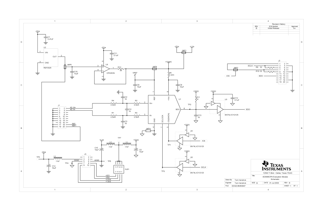
Texas Instruments MSOP8 manual Ti a

MSOP8 specifications

Texas Instruments MSOP8: An Overview of Features and Technologies

The Texas Instruments MSOP8, or Mini Small Outline Package 8, is a compact, dual-in-line package designed to house various analog and digital ICs. This package format facilitates tighter designs and is particularly suitable for applications where space is a critical constraint. With its compact dimensions of approximately 3.0 mm x 4.0 mm, the MSOP8 is favored in consumer electronics, automotive, and communication devices.

One of the primary features of the MSOP8 package is its low-profile design. The package height is typically around 0.75 mm, making it ideal for applications where height restrictions are paramount. This feature is especially beneficial in portable devices, where engineers must optimize space without sacrificing performance.

The MSOP8 package allows for a high level of integration. Manufacturers can implement multiple functions within a single chip, reducing the need for external components and aiding in overall circuit miniaturization. This characteristic not only streamlines the design process but also enhances reliability by minimizing interconnects and potential failure points.

Thermal performance is another notable aspect of the MSOP8. The construction of the package enables effective heat dissipation. This is crucial in high-performance applications where excessive heat can negatively impact functionality and longevity. Users can expect efficient thermal management from ICs housed in an MSOP8 package.

Texas Instruments has leveraged advanced manufacturing technologies and materials to enhance the reliability and performance of its MSOP8 offerings. Through the use of semiconductor technologies like CMOS (Complementary Metal-Oxide-Semiconductor) and BiCMOS (Bipolar CMOS), these devices deliver lower power consumption, higher speed, and increased functionality.

Electrical characteristics of the MSOP8 package contribute significantly to its versatility. Operating voltage ratings can vary across different devices, but many MSOP8 components are designed to work within a wide voltage range, providing flexibility in design. Input and output current ratings are typically robust, making this package suitable for driving loads in motor control and power management applications.

Furthermore, Texas Instruments ensures that MSOP8 components undergo rigorous testing and qualification processes to meet industry standards. This reliability makes the MSOP8 a preferred choice among engineers and designers working on mission-critical systems.

In conclusion, Texas Instruments' MSOP8 package stands out for its compact design, high level of integration, excellent thermal performance, and strong reliability. With its diverse applications across multiple sectors, the MSOP8 is a cornerstone in modern electronics, enabling innovative designs that meet the challenges of today’s market.