TAS5102, TAS5103EVM, TAS5103, TAS5102EVM specifications
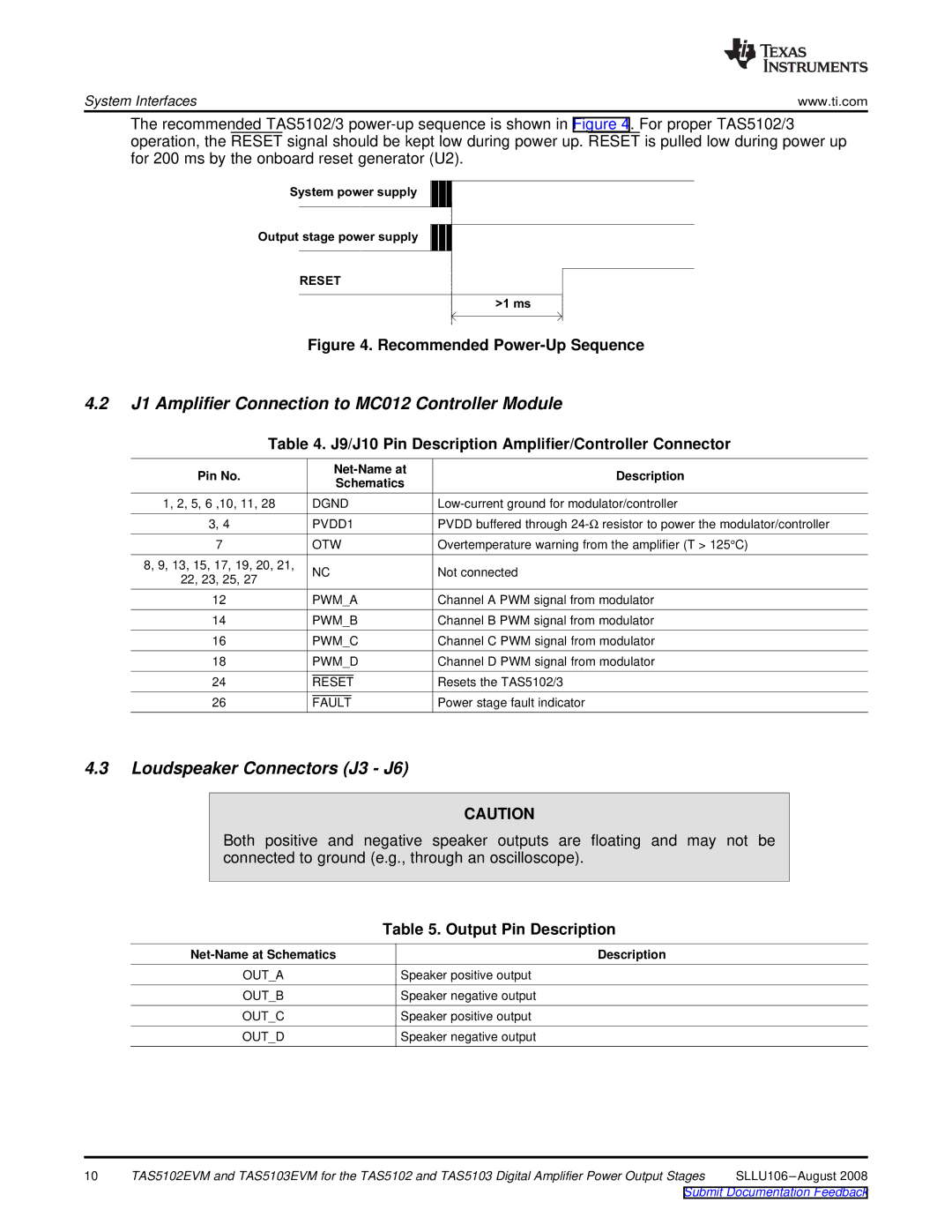
Texas Instruments (TI) has long been a leader in analog and embedded processing products, offering solutions that enhance audio quality and efficiency. Among their noteworthy offerings are the TAS5102 and TAS5103 digital amplifiers, as well as their corresponding evaluation modules, TAS5102EVM and TAS5103EVM. These products cater to audio professionals and enthusiasts looking for high-performance amplification solutions.The TAS5102 is a highly efficient digital audio amplifier designed for consumer and professional audio applications. Its primary feature is its ability to deliver robust power output while maintaining low total harmonic distortion (THD) and high signal-to-noise ratio (SNR). This amplifier architecture supports various digital audio formats, making it versatile for different sound applications. The integrated design allows it to support advanced features, such as automatic shut-off and thermal protection, ensuring safe operation without compromising performance.
On the other hand, the TAS5103 takes performance a step further with enhanced output power and thermal management, making it suitable for more demanding audio applications. It integrates a high-precision PWM modulator that greatly improves audio fidelity and expands the frequency response, allowing for a richer sound experience. The TAS5103 also features differential inputs, which help in reducing noise and achieving improved sound clarity.
The TAS5102EVM and TAS5103EVM evaluation modules provide developers with a platform to assess and implement the features of the TAS5102 and TAS5103 amplifiers. These modules offer extensive interfacing capabilities and flexibility for rapid prototyping. They come equipped with power management features and a user-friendly design, allowing engineers to focus on audio design without getting bogged down by the complexity of the underlying technology. The EVMs also provide real-time diagnostic tools, enabling users to monitor performance metrics and adjust settings on-the-fly, fostering an efficient development environment.
Both the TAS5102 and TAS5103 utilize cutting-edge technology, such as Class-D amplification, which offers significant power savings compared to traditional Class A or Class AB configurations. This technology not only reduces power consumption but also minimizes heat dissipation, extending the life of the audio components. With their compact design and high-performance characteristics, these amplifiers are ideal for applications in home theater systems, soundbars, and automotive audio systems, where quality sound is paramount.
In summary, the Texas Instruments TAS5102 and TAS5103, along with their respective EVMs, represent a powerful combination of innovative design and efficient performance, making them essential components for modern audio applications. With their focus on low distortion, high efficiency, and flexibility, these amplifiers are well-suited for capturing and delivering superior audio experiences.

