
TPS40003 specifications
The Texas Instruments TPS40003 is a versatile, high-performance synchronous buck controller designed to efficiently regulate output voltage in a range of applications. This device is particularly suited for power supply designs where space and efficiency are critical, such as telecommunications, industrial automation, and consumer electronics.One of the standout features of the TPS40003 is its ability to operate over a wide input voltage range of 4.5V to 36V. This flexibility allows it to be effectively utilized in various scenarios, accommodating different power supply systems and ensuring compatibility with existing infrastructure. Furthermore, the output voltage can be adjusted down to as low as 0.8V, making it suitable for powering low-voltage microcontrollers and FPGAs.
The TPS40003 incorporates advanced voltage mode control, which enhances transient response and stability. This control method allows for quick adjustments in duty cycle in response to load changes, ensuring a steady output voltage even under varying loads. Coupled with a programmable soft-start feature, the controller minimizes inrush current during startup, protecting sensitive downstream components.
Another significant advantage of the TPS40003 is its integration of a high-side and low-side MOSFET driver. This synchronous operation significantly improves power efficiency by reducing conduction losses. The device operates with a high switching frequency, typically around 200 kHz, allowing for the use of smaller passive components and ultimately leading to a more compact design.
Thermal performance is another essential characteristic of the TPS40003. With built-in thermal shutdown and overcurrent protection features, it promotes reliable operation under various thermal conditions, enhancing the overall robustness of the power supply design. Additionally, the device's wide range of compensation options allows designers to fine-tune performance according to specific application requirements.
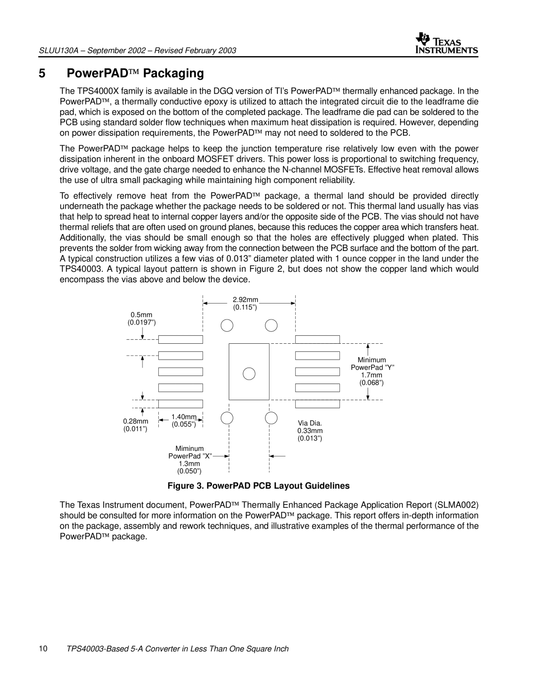
In terms of packaging, the TPS40003 is offered in a compact, thermally enhanced HTQFN package, which helps in conserving PCB space while maintaining efficient heat dissipation.
Overall, the Texas Instruments TPS40003 controller stands out as a robust, feature-rich solution for DC-DC conversion applications. With its wide operating voltage range, synchronous operation, and protective features, it provides designers with a reliable, efficient means of managing power in today's demanding electronic systems.