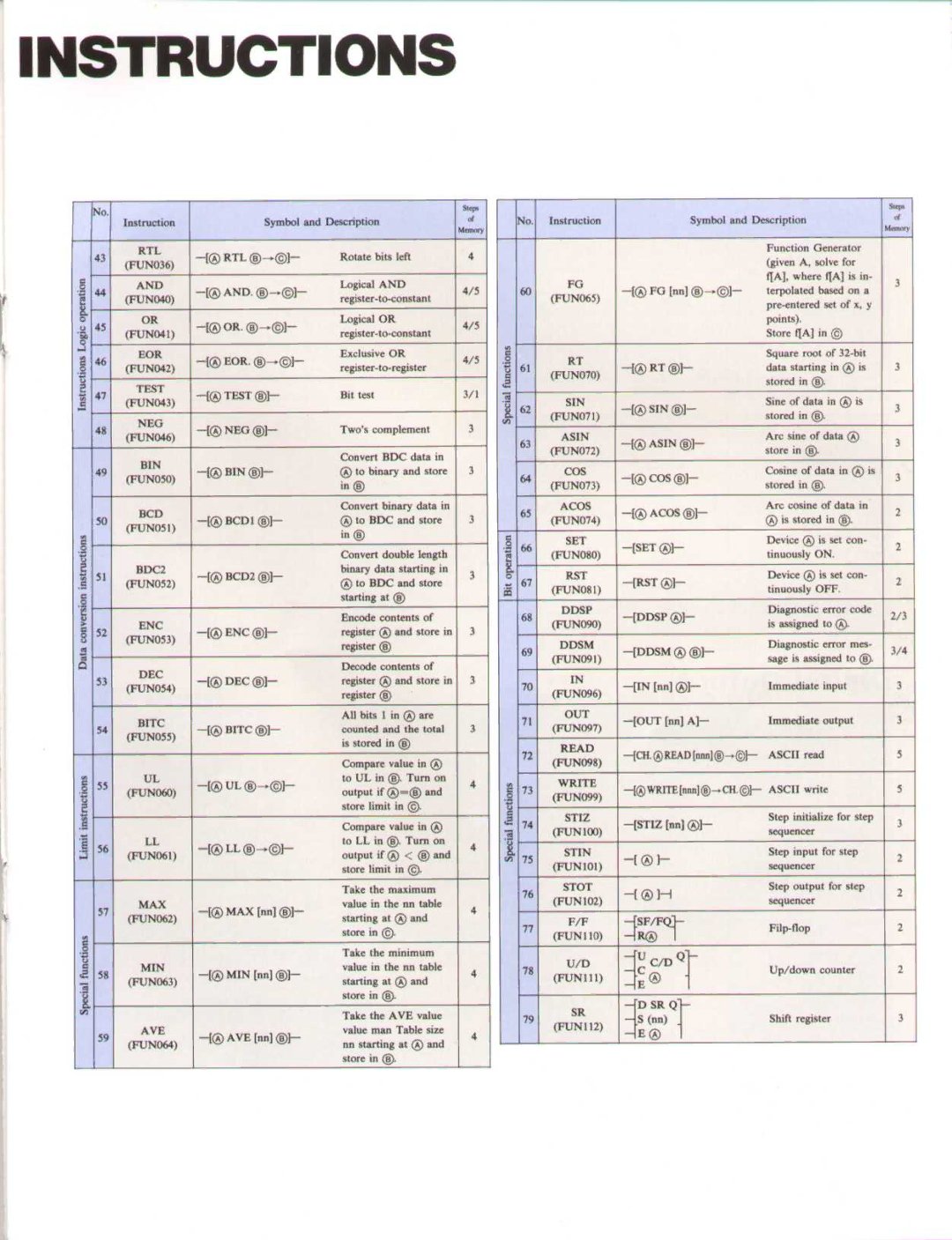
INSTRUCTIONS
No . | Instruction |
|
Symbol and Description | step" |
of | |
| Memory |
No. Instruction
Symbol and Description
step.
or
Memory
| 43 | RTL |
| (FUN036) | |
|
| |
| 44 | AND |
| (FUN040) | |
|
| |
Su | 45 | OR |
(FUN041) | ||
e | 46 | FOR |
o |
| (FUN042) |
2 |
| TEST |
-[O RTL
-[~ AND . 0~©]-
OR .
-[® EOR. 0 .©]-
Rotate bits left
Logical AND
Logical OR
Exclusive OR
4
4/5
4/5
4/5
60FG
(FUN065)
c |
|
| RT |
|
9 | 61 |
|
| |
o | ( | FUN070 | ) | |
,g |
|
|
-[® FG [nn]
-[~ RT ©]-
Function Generator (given A, solve for QA], where f[A] is in- terpolated based on a
Store f[A] in © Square root of
3
3
47 | (FUN043) |
|
48 | (FUN0G46) |
| |
| BIN |
49(FUNO50)
50BCD (FUN051)
51BDC2
(FUN052)
> | 52 | ENC |
| (FUN053) | |
|
|
-[O BIN ©]-
-[® BCD1 ©]-
BCD2 ©]-
- [0 ENC ©]-
Bit test
Two's complement
Convert BDC data in 0 to binary and store in ©
Convert binary data in 0 to BDC and store in ©
Convert double length binary data starting in to BDC and store
starting at 0 Encode contents of register 0 and store in register ®e
3/1
3
3
3
3
3
62 SIN
K(FUN071)
63 ASIN (FUN072)
64 | COS | |
(FUN073) | ||
| ||
65 | ACOS | |
| (FUN074) | |
66 | SET | |
(FUN080) | ||
$ |
| |
o 67 | RST | |
| (FUN081) | |
68 | DDSP | |
(FUN090) | ||
| ||
69 | DDSM | |
(FUN091) |
-[O SIN
[ n ASIN a _
- ~]
-[O COS O]-
-[O ACOS ©]-
-[SET ~]-
-[RST ~]-
-[DDSP 0]-
-[DDSM 0 ©]-
Sine of data in ® is stored in ©.
Arc sine of data ® store in © .
Cosine of data in 0 is stored in ®.
Arc cosine of data in 0 is stored in © . Device is set con- tinuously ON . Device 0 is set con- tinuously OFF .
Diagnostic error code is assigned to ®.
Diagnostic error mes- sage is assigned to ~.
3
3
3
2
2
2
2/3
3/4
A | 53 | DEC |
| ||
| (FUN054) | |
|
| |
| 54 | BITC |
| (FUN055) | |
|
|
-[O DEC ®]-
-[Oq BITC ©]-
Decode contents of register 0 and store in register ®
All bits I in 0 are counted and the total is stored in ©
Compare value in ®
3
3
70 | IN | |
(FUN096) | ||
| ||
71 | OUT | |
| (FUN097) | |
72 | READ | |
(FUN098) | ||
|
Immediate input
Immediate output
ASCII read
3
3
5
c | 55 | UL |
(FUN060) | ||
U |
|
|
y |
|
|
.E= | 56 | LL |
.a | (FUN061) |
57MAX
(FUN062)
°
58MIN
(FUN063)
59AVE (FUN064)
-[~ LL ©~©] _
- a MAX [nn] @)1- [~
-[~ MIN [nn] ~]-
-[® AVE [nn] ©]-
to UL in ®e . Turn on output if 0=0 and store limit in ©.
Compare value in 0 to LL in ©e . Turn on output if (D < © and store limit in © .
Take the maximum value in the nn table starting at 0 and store in ©.
Take the minimum value in the nn table starting at 0 and store in ®.
Take the AVE value value man Table size
nnstarting at 0 and store in © .
4
4
4
4
4
c | 73 | WRITE | |
(UN099) | |||
v | 74 | STIZ | |
a | |||
(FUNI00) |
75STIN
(FUNI01)
76STOT (FUN102)
77F/F
(FUN 110)
78U/D
(FUN 1 11)
79SR
(FUNI12)
Step initialize for step | ||
sequencer | ||
Step input for step | ||
sequences | ||
Step output for step | ||
| sequencer | |
SF/F | ||
IR® I | ||
| ||
CU C/D Q | Up/down counter | |
E n | ||
| ||
JD SRQ | Shift register | |
S (nn) | ||
E |
|
5
3
2
2
2
2
3