ZXLD1350EV2
ZXLD1350EV2 Evaluation Board.
Ref | Value | Package | Part Number | Manufacturer | Notes |
|
|
|
|
|
|
RS | 0.33R | 0805 | NCST10FR330FTRF | NIC |
|
| 1%,200ppm |
|
| components |
|
R1,R2 | Not fitted | 0805 |
|
| Not fitted |
C1,C2 | 1uF, 50V | 1206 | 50V, 1206 X7R | NIC |
|
|
|
| NMC1206X7R105K50F | components |
|
C3 | Not fitted | 0805 |
|
| Not fitted |
L1 | 100uH |
| NPIS53D101MTRF | NIC | 100uH/0.5A rms |
|
|
|
| components | Inductor |
SD1 | 40V, 1.16A | SOT23 | ZLLS1000 | Zetex | Schottky diode |
U1 | ZXLD1350 | ZXLD1350E5TA | Zetex | ||
D1, D2, D3 | 1W LED |
| Lumileds | 1W power LED | |
JP1, JP2, | Jumper |
|
| Various | 2.54mm pitch |
JP3 |
|
|
|
| jumper pin strips |
+VIN, GND, | Test loop |
| Hughes |
| |
ADJ, LED a, |
|
|
|
|
|
LED k |
|
|
|
|
|
J1 | 6 way |
| TYCO |
| |
| connector |
|
|
|
|
The slugs of the
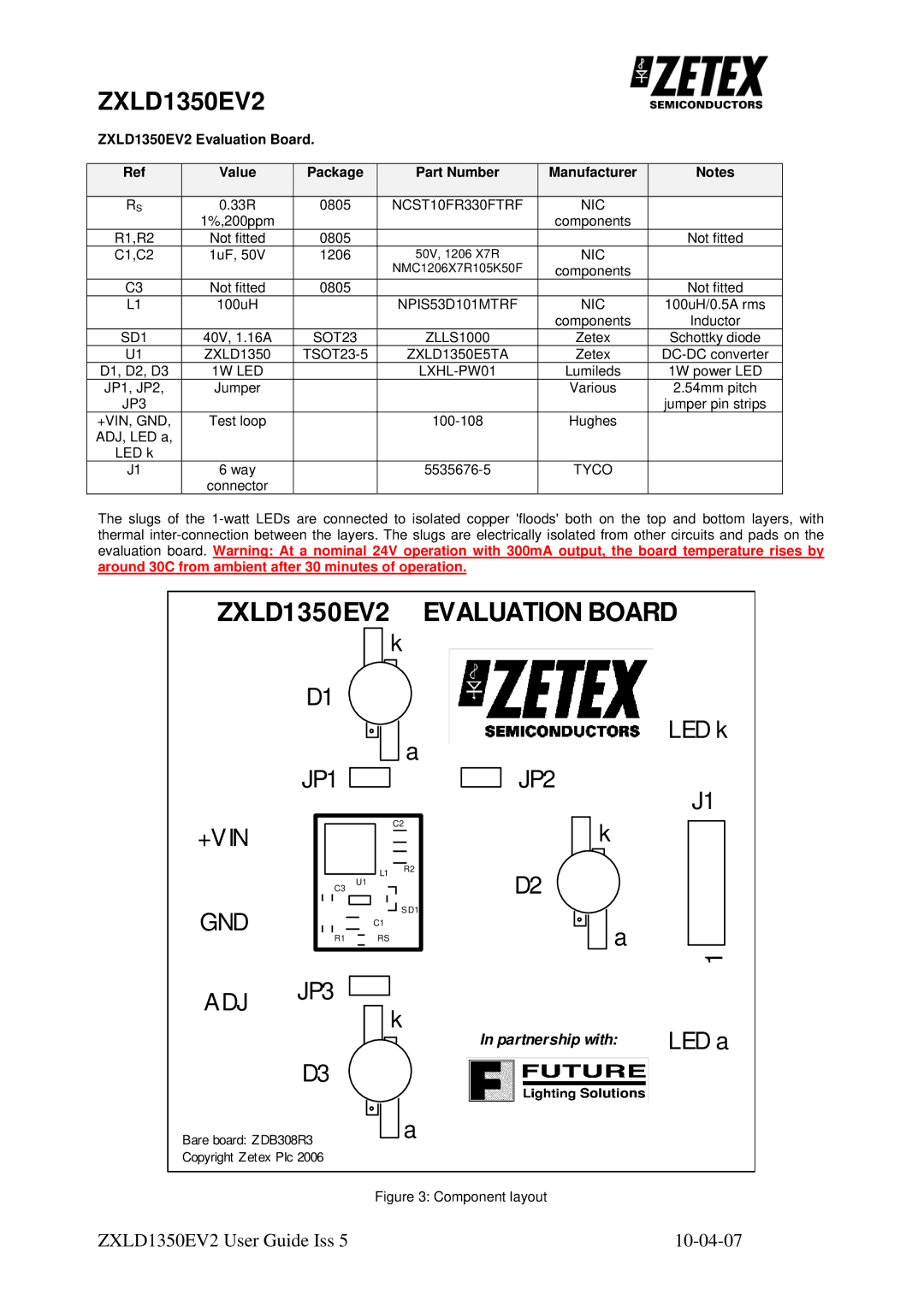
ZXLD1350EV2 EVALUATION BOARD
k
D1
a
JP1 ![]()
LED k
JP2
J1
+VIN
GND
C3
C2
L1 R2
U1
![]() SD1
SD1
C1
k
D2
R1 RS
a
1
ADJ JP3
D3
Bare board: ZDB308R3 Copyright Zetex Plc 2006
k
In partnership with: | LED a |
![]()
![]() a
a
Figure 3: Component layout
ZXLD1350EV2 User Guide Iss 5 |