ZXLD1350EV2
ZXLD1350EV2 EVALUATION BOARD
REFERENCE DESIGN
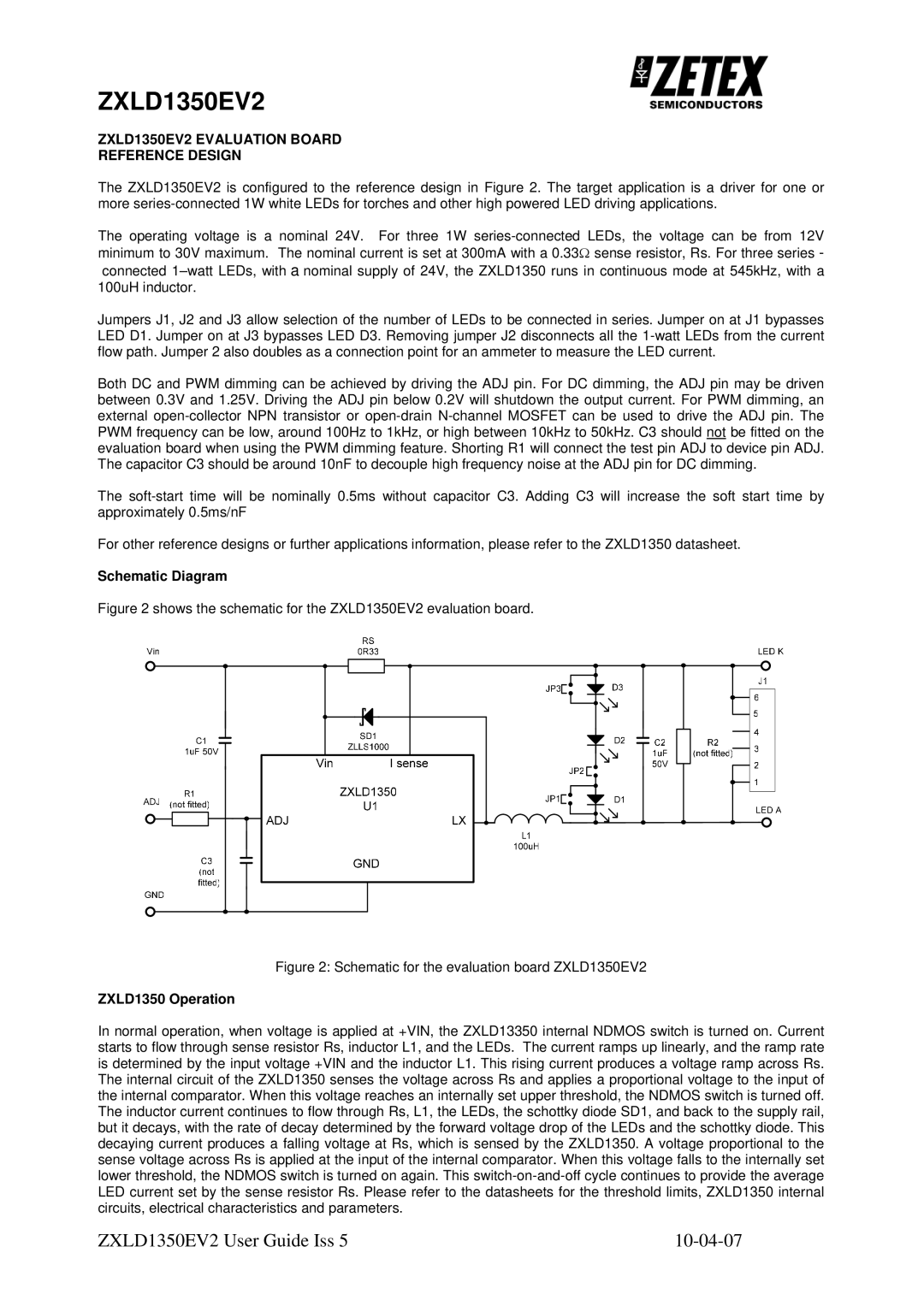
The ZXLD1350EV2 is configured to the reference design in Figure 2. The target application is a driver for one or more
The operating voltage is a nominal 24V. For three 1W
Jumpers J1, J2 and J3 allow selection of the number of LEDs to be connected in series. Jumper on at J1 bypasses LED D1. Jumper on at J3 bypasses LED D3. Removing jumper J2 disconnects all the
Both DC and PWM dimming can be achieved by driving the ADJ pin. For DC dimming, the ADJ pin may be driven between 0.3V and 1.25V. Driving the ADJ pin below 0.2V will shutdown the output current. For PWM dimming, an external
The
For other reference designs or further applications information, please refer to the ZXLD1350 datasheet.
Schematic Diagram
Figure 2 shows the schematic for the ZXLD1350EV2 evaluation board.
Figure 2: Schematic for the evaluation board ZXLD1350EV2
ZXLD1350 Operation
In normal operation, when voltage is applied at +VIN, the ZXLD13350 internal NDMOS switch is turned on. Current starts to flow through sense resistor Rs, inductor L1, and the LEDs. The current ramps up linearly, and the ramp rate is determined by the input voltage +VIN and the inductor L1. This rising current produces a voltage ramp across Rs. The internal circuit of the ZXLD1350 senses the voltage across Rs and applies a proportional voltage to the input of the internal comparator. When this voltage reaches an internally set upper threshold, the NDMOS switch is turned off. The inductor current continues to flow through Rs, L1, the LEDs, the schottky diode SD1, and back to the supply rail, but it decays, with the rate of decay determined by the forward voltage drop of the LEDs and the schottky diode. This decaying current produces a falling voltage at Rs, which is sensed by the ZXLD1350. A voltage proportional to the sense voltage across Rs is applied at the input of the internal comparator. When this voltage falls to the internally set lower threshold, the NDMOS switch is turned on again. This
ZXLD1350EV2 User Guide Iss 5 |