MB3842/MB3845
■PIN DESCRIPTION
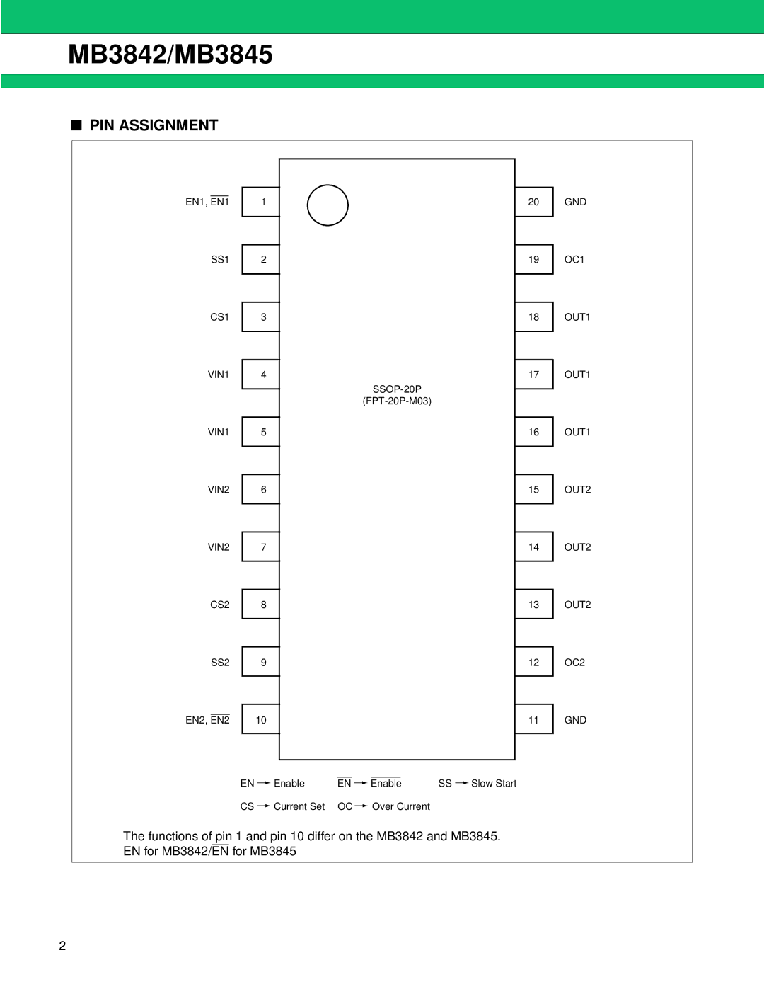
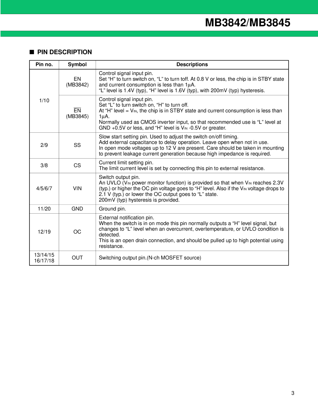
Pin no. | Symbol | Descriptions | |||
|
|
|
|
| |
|
|
|
| Control signal input pin. | |
|
| EN | Set “H” to turn switch on, “L” to turn toff. At 0.8 V or less, the chip is in STBY state | ||
| (MB3842) | and current consumption is less than 1∝A. | |||
|
|
|
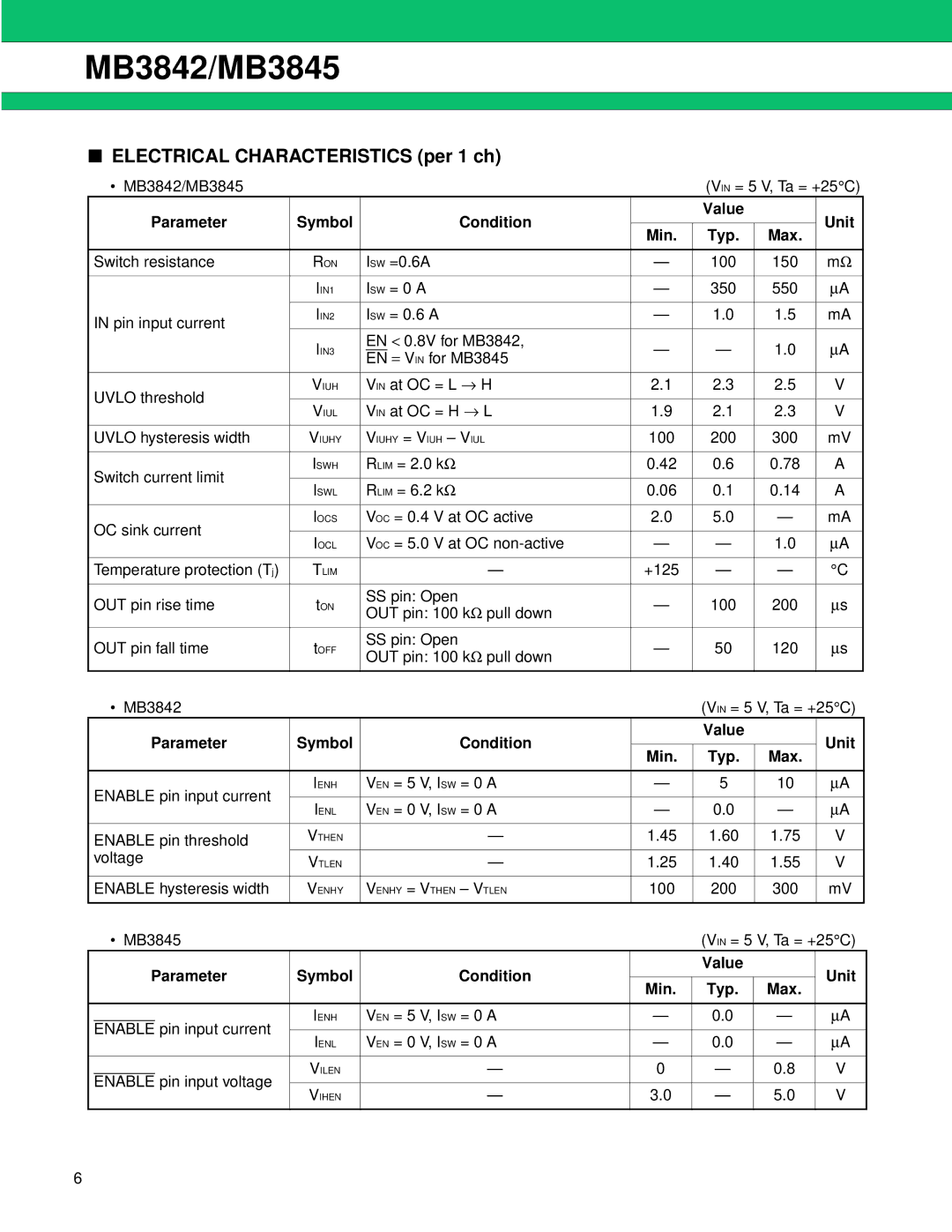
| “L” level is 1.4V (typ), “H” level is 1.6V (typ), with 200mV (typ) hysteresis. | |
|
|
|
|
| |
1/10 |
|
|
| Control signal input pin. | |
|
|
|
| Set “L” to turn switch on, “H” to turn off. | |
|
| EN |
| At “H” level = V IN, the chip is in STBY state and current consumption is less than | |
| (MB3845) | 1∝A. | |||
|
|
|
| Normally used as CMOS inverter input, so that recommended use is “L” level at | |
|
|
|
| GND +0.5V or less, and “H” level is V IN | |
|
|
|
|
| |
|
|
|
| Slow start setting pin. Used to adjust the switch on/off timing. | |
2/9 |
| SS | Add external capacitance to delay operation. Leave open when not in use. | ||
| In open mode voltages up to 12 V are present. Care should be taken in mounting | ||||
|
|
|
| ||
|
|
|
| to prevent leakage current generation because high impedance is required. | |
|
|
|
|
| |
3/8 |
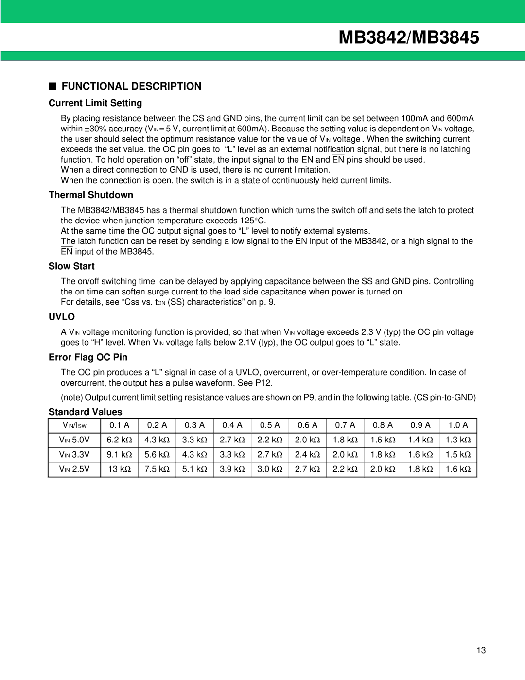
| CS | Current limit setting pin. | ||
| The limit current level is set by connecting this pin to external resistance. | ||||
|
|
|
| ||
|
|
|
|
| |
|
|
|
| Switch output pin. | |
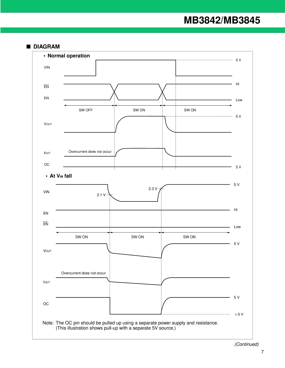
4/5/6/7 | VIN | An UVLO (VIN power monitor function) is provided so that when VIN reaches 2.3V | |||
(typ.) or higher the OC pin voltage goes to “H” level. Also if the V IN voltage drops to | |||||
|
|
|
| 2.1 V (typ.) or lower the OC output goes to “L” state. | |
|
|
|
| 200mV (typ) hysteresis is provided. | |
|
|
| |||
11/20 | GND | Ground pin. | |||
|
|
|
|
| |
|
|
|
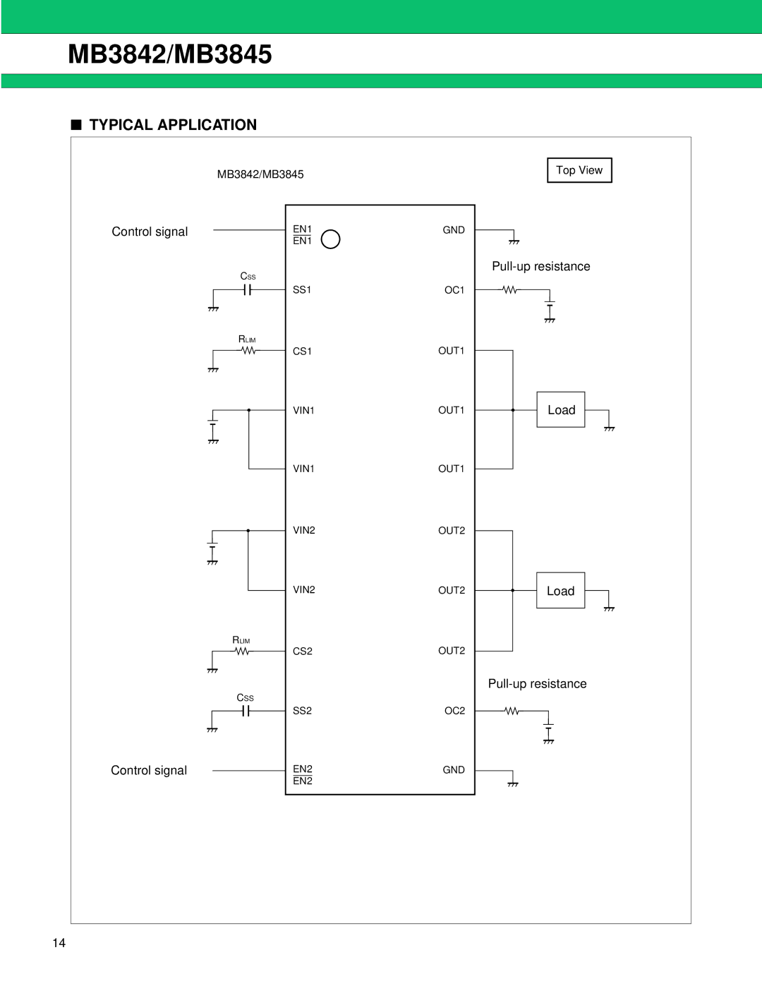
| External notification pin. | |
|
|
|
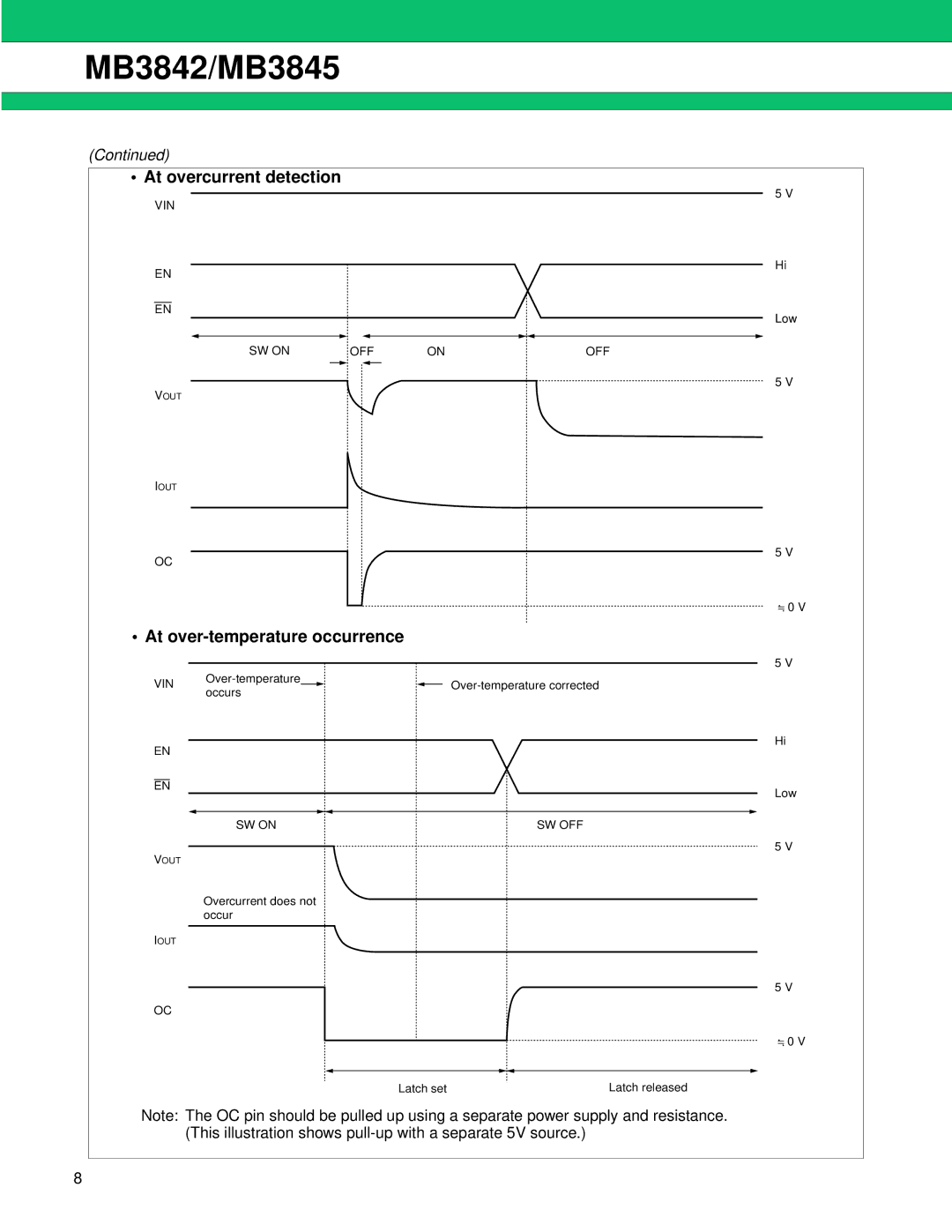
| When the switch is in on mode this pin normally outputs a “H” level signal, but | |
12/19 | OC | changes to “L” level when an overcurrent, overtemperature, or UVLO condition is | |||
detected. | |||||
|
|
|
| ||
|
|
|
| This is an open drain connection, and should be pulled up to high potential using | |
|
|
|
| resistance. | |
|
|
|
|
| |
13/14/15 | OUT | Switching output | |||
16/17/18 | |||||
|
|
|
| ||
|
|
|
|
| |
3
