Pin No. | Terminal | In/Out |
|
| Function | ||||||
|
|
|
|
|
|
|
|
|
|
|
|
106 | EOEB |
| Out |
| Read enable signal output for the effect RAM | ||||||
|
|
|
|
|
|
|
|
|
|
|
|
108 | VCC7 |
|
| In |
| +5V source | |||||
|
|
|
|
|
|
|
|
|
|
|
|
111 | ECEB |
| Out |
| Chip select signal output for the effect RAM | ||||||
|
|
|
|
|
|
|
|
|
|
|
|
113 ~ 117 | ED11 ~ ED15 |
|
|
|
|
|
| Not used | |||
|
|
|
|
| |||||||
|
|
|
|
|
|
|
|
|
|
|
|
118 | VCC4 |
|
| In |
| +5V source | |||||
|
|
|
|
|
|
|
|
|
|
|
|
119 | GND4 |
|
| In |
| Ground (0V) source | |||||
|
|
|
|
|
|
|
|
|
|
|
|
120 ~ 122 | ED8 ~ ED10 |
|
|
|
|
|
| Not used |
| ||
|
|
|
|
| |||||||
|
|
|
|
|
|
|
|
|
|
|
|
123 ~ 130 | ED0 ~ ED7 | In/Out |
| Data bus for the effect RAM | |||||||
|
|
|
|
|
|
|
|
|
|
|
|
131 | GND5 |
|
| In |
| Ground (0V) source | |||||
|
|
|
|
|
|
|
|
|
|
|
|
132 ~ 134 |
|
|
|
|
|
|
|
|
| Not used. Connected to ground. | |
|
|
|
|
|
|
|
| ||||
|
|
|
|
|
|
|
|
|
|
|
|
135, 136 |
|
|
|
|
|
|
|
|
| Not used | |
|
|
|
|
|
|
|
| ||||
|
|
|
|
|
|
|
|
|
|
|
|
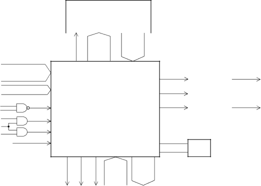
Block diagram of DSP and DAC circuit
D0 ~ D7
A0 ~ A3
A12
A14
RD
APO
WR
RESET
Sound Source ROM
LSI101
| CE A0 ~ A19 | D0 ~ D15 | ||
RA22 | RA0 ~ | RD0 ~ | ||
RA19 | RD15 | |||
|
| |||
|
|
| DSP |
| |
CCSB | LSI102 |
| |||
|
|
| |||
CRDB | HG51B155FD |
| |||
|
|
| |||
CWRB |
|
|
| ||
RESB |
|
|
| ||
ECEB EOEB EWEB |
| ||||
CS OE WE | ED0 ~ | EA0 ~ | |||
ED15 | EA14 | ||||
|
|
| |||
|
|
|
|
| |
|
|
| D0 ~ D15 | A0 ~ A14 | |
|
| Effect RAM | |||
|
|
| LSI103 |
| |
|
|
| |||
|
|
|
|
| |
SOLP: Sound data
BOK: Bit clock
WOK1: Word clock
| DAC |
|
SOLP | SI LSI104 | ROUT |
BOK | CLK |
|
|
| |
WOK1 | LRCK | LOUT |
|
| |
| UPD6376GS |
|
|
|
|
PG
X101
24.576 MHz
— 13 —