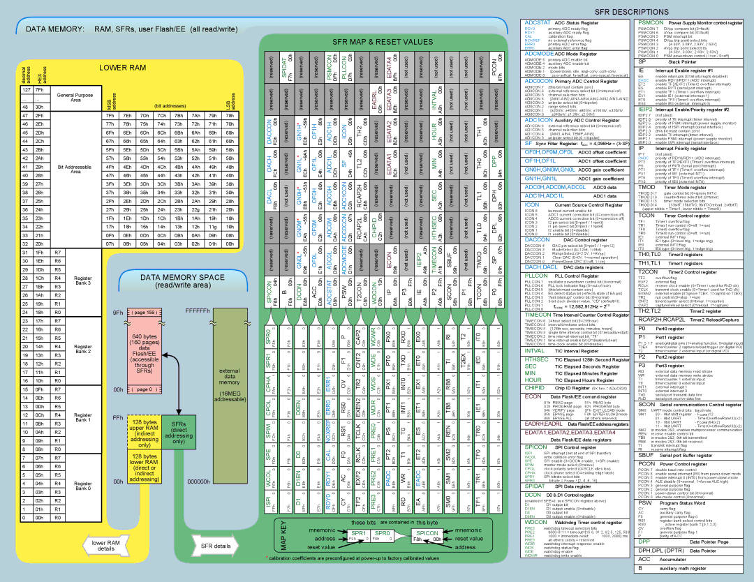
SFR DESCRIPTIONS
DATA MEMORY: RAM, SFRs, user Flash/EE (all read/write)
decimal address | HEX address |
|
| LOWER RAM |
|
|
|
|
| ||
|
|
|
|
|
|
|
|
|
| ||
127 | 7Fh | General Purpose | MSB address |
|
|
|
|
|
| LSB address | |
... | ... |
|
|
|
|
|
| ||||
| Area |
|
|
|
|
|
| ||||
|
|
|
|
|
|
|
|
| |||
48 | 30h |
|
|
|
| (bit addresses) |
| ||||
47 | 2Fh |
|
| 7Fh | 7Eh | 7Dh | 7Ch | 7Bh | 7Ah | 79h | 78h |
46 | 2Eh |
|
| 77h | 76h | 75h | 74h | 73h | 72h | 71h | 70h |
45 | 2Dh |
|
| 6Fh | 6Eh | 6Dh | 6Ch | 6Bh | 6Ah | 69h | 68h |
44 | 2Ch |
|
| 67h | 66h | 65h | 64h | 63h | 62h | 61h | 60h |
43 | 2Bh |
|
| 5Fh | 5Eh | 5Dh | 5Ch | 5Bh | 5Ah | 59h | 58h |
42 | 2Ah |
|
| 57h | 56h | 55h | 54h | 53h | 52h | 51h | 50h |
41 | 29h | Bit Addressable | 4Fh | 4Eh | 4Dh | 4Ch | 4Bh | 4Ah | 49h | 48h | |
40 | 28h |
| Area | 47h | 46h | 45h | 44h | 43h | 42h | 41h | 40h |
|
| ||||||||||
39 | 27h |
|
| 3Fh | 3Eh | 3Dh | 3Ch | 3Bh | 3Ah | 39h | 38h |
38 | 26h |
|
| 37h | 36h | 35h | 34h | 33h | 32h | 31h | 30h |
37 | 25h |
|
| 2Fh | 2Eh | 2Dh | 2Ch | 2Bh | 2Ah | 29h | 28h |
36 | 24h |
|
| 27h | 26h | 25h | 24h | 23h | 22g | 21h | 20h |
35 | 23h |
|
| 1Fh | 1Eh | 1Dh | 1Ch | 1Bh | 1Ah | 19h | 18h |
34 | 22h |
|
| 17h | 16h | 15h | 14h | 13h | 12h | 11g | 10h |
33 | 21h |
|
| 0Fh | 0Eh | 0Dh | 0Ch | 0Bh | 0Ah | 09h | 08h |
32 | 20h |
|
| 07h | 06h | 05h | 04h | 03h | 02h | 01h | 00h |
31 | 1Fh | R7 |
|
|
|
|
|
|
|
|
|
30 | 1Eh | R6 |
|
|
|
|
|
|
|
|
|
29 | 1Dh | R5 |
|
|
| DATA MEMORY SPACE |
| ||||
28 | 1Ch | R4 | Register |
|
|
| |||||
27 | 1Bh | R3 | Bank 3 |
|
|
| (read/write area) |
| |||
|
|
|
|
| |||||||
26 | 1Ah | R2 |
|
|
|
|
|
|
|
|
|
25 | 19h | R1 |
|
|
|
|
|
|
|
|
|
24 | 18h | R0 |
| 9Fh |
| ( page 159 ) |
| FFFFFFh |
| ||
|
|
|
|
|
| ||||||
23 | 17h | R7 |
|
|
|
|
|
|
|
|
|
SFR MAP & RESET VALUES
(reserved) |
| SPIDAT | F7h 00h | (reserved) |
| (reserved) |
| PSMCON | DFh DEh | PLLCON | D7h 03h | (reserved) |
| (reserved) |
| EDATA4 | BFh 00h | (not used) | (reserved) |
| (not used) |
| (not used) |
| (not used) | (reserved) |
| PCON | 87h 00h |
|
|
|
|
|
|
|
|
|
|
|
|
|
|
|
|
|
|
|
|
|
|
|
|
|
|
|
|
|
|
(reserved) |
| (reserved) |
| (reserved) |
| (reserved) |
| (reserved) |
| (reserved) |
| (reserved) |
| EADRL | C6h 00h | EDATA3 | BEh 00h | (reserved) | (reserved) |
| INTVAL | A6h 00h | (not used) |
| (not used) | (reserved) |
| (reserved) |
|
|
|
|
|
|
|
|
|
|
|
|
|
|
|
|
|
|
|
|
|
|
|
|
|
|
|
|
|
|
|
DACCON | FDh 00h | (reserved) |
| GN1H* | EDh ~59h | OF1H | E5h 80h | ADC1H | DDh 00h | ICON | D5h 00h | TH2 | CDh 00h | (reserved) |
| EDATA2 | BDh 00h | (reserved) | (reserved) |
| HOUR | A5h 00h | (not used) |
| (not used) | TH1 | 8Dh 00h | (reserved) |
|
|
|
|
|
|
|
|
|
|
|
|
|
|
|
|
|
|
|
|
|
|
|
|
|
|
|
|
|
|
|
DACH | FCh 00h | (reserved) |
| GN1L* | ECh ~9Ah | OF1L | E4h 00h | ADC1L | DCh 00h | SF | D4h 45h | TL2 | CCh 00h | (reserved) |
| EDATA1 | BCh 00h | (not used) | (reserved) |
| MIN | A4h 00h | (not used) |
| (not used) | TH0 | 8Ch 00h | DPP | 84h 00h |
|
|
|
|
|
|
|
|
|
|
|
|
|
|
|
|
|
|
|
|
|
|
|
|
|
|
|
|
|
|
DACL | FBh 00h | (not used) |
| GN0H* | EBh ~53h | OF0H | E3h 80h | ADC0H | DBh 00h | ADC1CON | D3h 00h | RCAP2H | CBh 00h | (reserved) |
| (reserved) |
| (not used) | (reserved) |
| SEC | A3h 00h | (reserved) |
| (not used) | TL1 | 8Bh 00h | DPH | 83h 00h |
|
|
|
|
|
|
|
|
|
|
|
|
|
|
|
|
|
|
|
|
|
|
|
|
|
|
|
|
|
|
(reserved) |
| (reserved) |
| GN0M* | EAh ~55h | OF0M | E2h 00h | ADC0M | DAh 00h | ADC0CON | D2h 07h | RCAP2L | CAh 00h | CHIPID | C2h 06h | (reserved) |
| (not used) | (reserved) |
| HTHSEC | A2h 00h | (reserved) |
| (not used) | TL0 | 8Ah 00h | DPL | 82h 00h |
|
|
|
|
|
|
|
|
|
|
|
|
|
|
|
|
|
|
|
|
|
|
|
|
|
|
|
|
|
|
(reserved) |
| (reserved) |
| GN0L* | E9h ~55h | OF0L | E1h 00h | ADC0L | D9h 00h | ADCMODE | D1h 00h | (reserved) |
| (reserved) |
| ECON | B9h 00h | (not used) | IEIP2 | A9h A0h | TIMECON | A1h 00h | SBUF | 99h 00h | (not used) | TMOD | 89h 00h | SP | 81h 07h |
|
|
|
|
|
|
|
|
|
|
|
|
|
|
|
|
|
|
|
|
|
|
|
|
|
|
|
|
|
|
SPICON | F8h 04h | B | F0h 00h | DCON | E8h 00h | ACC | E0h 00h | ADCSTAT | D8h 00h | PSW | D0h 00h | T2CON | C8h 00h | WDCON | C0h 10h | IP | B8h 00h | P3 B0h FFh | IE | A8h 00h | P2 | A0h FFh | SCON | 98h 00h | P1 90h FFh | TCON | 88h 00h | P0 | 80h FFh |
|
|
|
|
|
|
|
|
|
|
|
|
|
|
|
|
|
|
|
|
|
|
|
|
|
|
|
|
|
|
ADCSTAT ADC Status Register
RDY0 | primary ADC ready flag |
RDY1 | auxiliary ADC ready flag |
CAL | calibration flag |
NOXREF | no external reference flag |
ERR0 | primary ADC error flag |
ERR1 | auxiliary ADC error flag |
ADCMODE ADC Mode Register | |
ADMODE.5 | primary ADC enable bit |
ADMODE.4 | auxiliary ADC enable bit |
ADMODE.2 | mode bits |
ADMODE.1 | [powerdown, idle, |
ADMODE.0 | |
ADC0CON Primary ADC Control Register | |
AD0CON.7 | (this bit must contain zero) |
AD0CON.6 | external reference select bit (0=internal ref) |
AD0CON.5 | channel selection bits: |
AD0CON.4 | |
AD0CON.3 | unipolar select bit (0=bipolar) |
AD0CON.2 | range select bits: |
AD0CON.1 | [±20mV, ±40mV, ±80mV, ±160mV, ±320mV, |
AD0CON.0 | ±640mV, ±1.28V, ±2.56V] |
ADC1CON Auxiliary ADC Control Register | |
AD1CON.6 | external reference select bit (0=internal ref) |
AD1CON.5 | channel selection bits: |
AD1CON.4 | [AIN3, AIN4, TEMP, AIN5] |
AD1CON.3 | unipolar select bit (0 = bipolar) |
SF Sync Filter Register: fADC = 4,096Hz ÷ (3·SF)
OF0H,OF0M,OF0L | ADC0 offset coefficient | ||
|
| ||
OF1H,OF1L | ADC1 offset coefficient | ||
| |||
GN0H,GN0M,GN0L ADC0 gain coefficient | |||
|
| ||
GN1H,GN1L | ADC1 gain coefficient | ||
| |||
ADC0H,ADC0M,ADC0L ADC0 data | |||
|
| ||
ADC1H,ADC1L | ADC1 data | ||
|
|
| |
ICON |
| Current Source Control Register | |
ICON.6 | burnout current enable bit | ||
ICON.5 | ADC1 current correction bit (0=correction off) | ||
ICON.4 | ADC0 current correction bit (0=correction off) | ||
ICON.3 | I2 pin select bit [0=pin4 / 1=pin3] | ||
ICON.2 | I1 pin select bit [0=pin3 / 1=pin4] | ||
ICON.1 | I2 enable bit (0=disable) | ||
ICON.0 | I1 enable bit (0=disable) | ||
DACCON | DAC Control register | ||
DACCON.4 |
| DAC pin select bit [0=pin3 / 1=pin12] | |
DACCON.3 |
| ModeSelect (0=12bit, 1=8bit) | |
DACCON.2 |
| RangeSelect (0=2.5V, 1=AVDD) | |
DACCON.1 |
| Clear DAC (0=0V, 1=normal operation) | |
DACCON.0 |
| PowerDown DAC (0=off, 1=on) | |
DACH,DACL DAC data registers | |||
|
|
| |
PLLCON |
| PLL Control Register | |
PLLCON.7 | oscillator powerdown control bit (0=normal) | ||
PLLCON.6 | PLL lock indicator flag (0=out of lock) | ||
PLLCON.5 | (this bit must contain zero) | ||
PLLCON.4 | EA detect status bit (reflects state of EA pin) | ||
PLLCON.3 | “fast interrupt” control bit (0=normal) | ||
PLLCON.2 | |||
PLLCON.1 |
| fCORE = 12,582,912Hz ÷ 2CD | |
PLLCON.0 |
|
|
|
TIMECON Time Interval Counter Control Register | |||
TIMECON.6 | 24hour select bit (0=255hour) | ||
TIMECON.5 | interval timebase select bits | ||
PSMCON Power Supply Monitor control register
PSMCON.7 | DVDD compare bit (0=fault) | |
PSMCON.6 | AVDD compare bit (0=fault) | |
PSMCON.5 | PSM interrupt bit | |
PSMCON.4 | DVDD trip point select bits | |
PSMCON.3 | [4.63V, 3.08V, 2.93V, 2.63V] | |
PSMCON.2 | AVDD trip point select bits | |
PSMCON.1 | [4.63V, 3.08V, 2.93V, 2.63V] | |
PSMCON.0 | PSM powerdown control (1=on / 0=off) | |
SP |
| Stack Pointer |
|
| |
IE | Interrupt Enable register #1 | |
EA | enable inturrupts (0=all inturrupts disabled) | |
EADC | enable RDY0/RDY1 (ADC interrupt) | |
ET2 | enable TF2/EXF2 (Timer2 overflow interrupt) | |
ES | enable RI/TI (serial port interrupt) | |
ET1 | enable TF1 (Timer1 overflow interrupt) | |
EX1 | enable IE1 (external interrupt 1) | |
ET0 | enable TF0 (Timer0 overflow interrupt) | |
EX0 | enable IE0 (external interrupt 0) | |
IEIP2 | Interrupt Enable/Priority register #2 | |
IEIP2.7 | (not used) | |
IEIP2.6 | pirority of TII interrupt (timer interval) | |
IEIP2.5 | priority of PSMI interrupt (power supply monitor) | |
IEIP2.4 | priority of ISPI interrupt (serial interface) | |
IEIP2.3 | (this bit must contain zero) | |
IEIP2.2 | enable TII interrupt (timer interval) | |
IEIP2.1 | enable PSMI interrupt (power supply monitor) | |
IEIP2.0 | enable ISPI interrupt (serial interface) | |
IP | Interrupt Priority register | |
IP.7 | (not used) | |
PADC | priority of RDY0/RDY1 (ADC interrupt) | |
PT2 | priority of TF2/EXF2 (Timer2 overflow interrupt) | |
PS | priority of RI/TI (serial port interrupt) | |
PT1 | priority of TF1 (Timer1 overflow interrupt) | |
PX1 | priority of IE1 (external INT1) | |
PT0 | priority of TF0 (Timer0 overflow interrupt) | |
PX0 | priority of IE0 (external INT0) | |
TMOD |
| Timer Mode register |
TMOD.3/.7 | gate control bit (0=ignore INTx) | |
TMOD.2/.6 | counter/timer select bit (0=timer) | |
TMOD.1/.5 | timer mode selecton bits | |
TMOD.0/.4 | [13bitT, 16bitT/C, 8bitT/Creload, 2x8bitT] | |
(upper nibble = Timer1, lower nibble = Timer0) | ||
TCON |
| Timer Control register |
TF1 | Timer1 overflow flag | |
TR1 | Timer1 run control (0=off, 1=run) | |
TF0 | Timer0 overflow flag | |
TR0 | Timer0 run control (0=off, 1=run) | |
IE1 | external INT1 flag | |
IT1 | IE1 type (0=level trig, 1=edge trig) | |
IE0 | external INT0 flag | |
IT0 | IE0 type (0=level trig, 1=edge trig) | |
TH0,TL0 | Timer0 registers | |
|
| |
TH1,TL1 | Timer1 registers | |
|
| |
T2CON | Timer2 Control register | |
TF2 | overflow flag | |
EXF2 | external flag | |
RCLK | receive clock enable (0=Timer1 used for RxD clk) | |
TCLK | transmit clock enable (0=Timer1 used for TxD clk) | |
EXEN2 | external enable (0=ignore T2EX, 1=cap/rld on T2EX) | |
TR2 | run control (0=stop, 1=run) | |
CNT2 | timer/counter select (0=timer, 1=counter) | |
CAP2 | capture/reload select (0=reload, 1=capture) | |
TH2,TL2 | Timer2 register | |
RCAP2H,RCAP2L Timer2 Reload/Capture
22 | 16h | R6 |
|
|
|
|
|
|
|
|
|
|
|
|
|
| 640 bytes |
|
|
| |
21 | 15h | R5 |
|
|
|
|
|
| ||
|
|
|
|
|
| (160 pages) |
|
|
| |
20 | 14h | R4 | Register |
|
| data |
|
|
|
|
19 | 13h | R3 | Bank 2 |
|
| Flash/EE |
|
|
|
|
|
|
|
|
|
| (accessible |
|
|
| |
18 | 12h | R2 |
|
|
| through |
|
|
|
|
17 | 11h | R1 |
|
|
| SFRs) |
|
|
| external |
|
|
|
|
|
|
|
|
|
| data |
16 | 10h | R0 |
|
|
|
|
|
|
| memory |
15 | 0Fh | R7 |
| 00h | ( page 0 | ) |
|
| (16MEG | |
14 | 0Eh | R6 |
|
|
|
|
|
|
| addressable) |
13 | 0Dh | R5 |
|
|
|
|
|
|
|
|
|
|
|
|
|
|
|
|
|
|
|
12 | 0Ch | R4 | Register | FFh |
|
|
|
|
| |
11 | 0Bh | R3 | Bank 1 |
|
| 128 bytes | SFRs |
|
| |
|
|
| upper RAM |
|
| |||||
|
|
|
|
|
| (direct |
|
| ||
10 | 0Ah | R2 |
|
|
|
|
| |||
|
|
| (indirect |
|
|
| ||||
|
|
|
| addressing |
|
| ||||
9 | 09h | R1 |
|
|
| addressing | only) |
|
| |
|
|
| only) |
|
|
| ||||
8 | 08h | R0 |
|
|
|
|
|
|
| |
7 | 07h | R7 |
|
|
| 128 bytes |
|
|
| |
|
|
|
|
|
| lower RAM |
|
|
| |
6 | 06h | R6 |
|
|
| (direct or |
|
|
| |
5 | 05h | R5 |
|
|
| indirect |
|
|
|
|
|
|
|
| 00h | addressing) | 000000h |
| |||
4 | 04h | R4 | Register |
| ||||||
|
|
| ||||||||
|
|
| Bank 0 |
|
|
|
|
|
|
|
3 | 03h | R3 |
|
|
|
|
|
|
| |
|
|
|
|
|
|
|
| |||
|
|
|
|
|
|
|
|
|
|
|
2 | 02h | R2 |
|
|
|
|
|
|
|
|
|
|
|
|
|
|
|
|
|
|
|
1 | 01h | R1 |
|
|
|
|
|
|
|
|
|
|
|
|
|
|
|
|
|
|
|
0 | 00h | R0 |
|
|
|
|
|
|
|
|
SPR0 | 0 |
F8h | |
|
|
SPR1 | 0 |
F9h | |
|
|
CPHA | FAh 1 |
|
|
CPOL | FBh 0 |
|
|
SPIM | 0 |
FCh | |
|
|
SPE | 0 |
FDh | |
|
|
WCOL | FEh 0 |
|
|
| 0 |
ISPI | FFh |
F7h 0 F6h 0 F5h 0 F4h 0 F3h 0 F2h 0 F1h 0 F0h 0![]()
![]()
| 0 |
| E8h |
| 0 |
| E9h |
| 0 |
| EAh |
D0EN | EBh 0 |
| 0 |
| ECh |
| 0 |
D0 | EDh |
D1EN | EEh 0 |
| 0 |
D1 | EFh |
E7h 0 E6h 0 E5h 0 E4h 0 E3h 0 E2h 0 E1h 0 E0h 0![]()
![]()
| 0 |
| D8h |
| 0 |
| D9h |
ERR1 | DAh 0 |
ERR0 | DBh 0 |
NOXREF | DCh 0 |
| 0 |
CAL | DDh |
RDY1 | DEh 0 |
RDY0 | DFh 0 |
| 0 |
P | D0h |
| |
|
|
| 0 |
F1 | D1h |
|
|
| 0 |
OV D2h | |
|
|
RS0 | 0 |
D3h | |
|
|
RS1 | 0 |
D4h | |
|
|
| 0 |
F0 | D5h |
|
|
| 0 |
AC D6h | |
|
|
| 0 |
CY D7h | |
CAP2 | 0 |
C8h | |
|
|
CNT2 | 0 |
C9h | |
|
|
| 0 |
TR2 | CAh |
|
|
EXEN2 | CBh 0 |
|
|
TCLK | 0 |
CCh | |
|
|
RCLK | 0 |
CDh | |
|
|
EXF2 | 0 |
CEh | |
|
|
| 0 |
TF2 | CFh |
WDWR | C0h 0 |
|
|
WDE | 0 |
C1h | |
|
|
WDS | 0 |
C2h | |
|
|
WDIR | C3h 0 |
|
|
PRE0 | 1 |
C4h | |
|
|
PRE1 | 0 |
C5h | |
|
|
PRE2 | 0 |
C6h | |
|
|
PRE3 | 0 |
C7h |
| 0 |
PX0 | B8h |
|
|
| 0 |
PT0 | B9h |
|
|
| 0 |
PX1 | BAh |
|
|
| 0 |
PT1 | BBh |
|
|
| 0 |
PS BCh | |
|
|
| 0 |
PT2 | BDh |
|
|
PADC | BEh 0 |
|
|
| 0 |
| BFh |
RXD | 1 |
B0h | |
|
|
TXD | 1 |
B1h | |
|
|
INT0 | 1 |
B2h | |
|
|
INT1 | 1 |
B3h | |
|
|
| 1 |
T0 | B4h |
|
|
| 1 |
T1 | B5h |
|
|
| 1 |
WR B6h | |
|
|
| 1 |
RD B7h | |
| 0 |
EX0 | A8h |
|
|
| 0 |
ET0 | A9h |
|
|
| 0 |
EX1 | AAh |
|
|
| 0 |
ET1 | ABh |
|
|
| 0 |
ES ACh | |
|
|
| 0 |
ET2 | ADh |
|
|
EADC | AEh 0 |
|
|
| 0 |
EA AFh | |
A7h 1 A6h 1 A5h 1 A4h 1 A3h 1 A2h 1 A1h 1 A0h 1![]()
![]()
| 0 |
RI | 98h |
| |
| 0 |
TI | 99h |
| 0 |
RB8 | 9Ah |
| 0 |
TB8 | 9Bh |
REN | 0 |
9Ch | |
SM2 | 0 |
9Dh | |
SM1 | 0 |
9Eh | |
SM0 | 0 |
9Fh |
| 1 |
T2 | 90h |
|
|
T2EX | 1 |
91h | |
|
|
| 1 |
| 92h |
|
|
| 1 |
| 93h |
|
|
| 1 |
| 94h |
|
|
| 1 |
| 95h |
|
|
| 1 |
| 96h |
|
|
| 1 |
| 97h |
| 0 |
IT0 | 88h |
| 0 |
IE0 | 89h |
| 0 |
IT1 | 8Ah |
| 0 |
IE1 | 8Bh |
| 0 |
TR0 | 8Ch |
| 0 |
TF0 | 8Dh |
| 0 |
TR1 | 8Eh |
| 0 |
TF1 | 8Fh |
87h 1 86h 1 85h 1 84h 1 83h 1 82h 1 81h 1 80h 1
TIMECON.4 |
| [128th sec, seconds, minutes, hours] | |
TIMECON.3 | single time interval control bit (0=reload&restart) | ||
TIMECON.2 | time interval interrupt bit, “TII” | ||
TIMECON.1 | time interval enable bit (0=disable&clear) | ||
TIMECON.0 | time clock enable bit (0=disable) | ||
INTVAL |
| TIC Interval Register | |
|
|
| |
HTHSEC |
| TIC Elapsed 128th Second Register | |
SEC |
| TIC Elapsed Seconds Register | |
MIN |
| TIC Elapsed Minutes Register | |
HOUR |
| TIC Elapsed Hours Register | |
|
|
| |
CHIPID |
| Chip ID Register (0X hex = ADuC824) | |
|
|
| |
ECON |
| Data Flash/EE comand register | |
01h READ page | 81h READ byte | ||
02h PROGRAM page | 82h PROGRAM byte | ||
04h | VERIFY page | 0Fh EXIT ULOAD mode | |
05h | ERASE page | F0h ENTER ULOAD mode | |
06h | ERASE ALL | (all others reserved) | |
EADRH,EADRL Data Flash/EE address registers
EDATA1,EDATA2,EDATA3,EDATA4
|
| Data Flash/EE data registers |
SPICON | SPI Control register | |
ISPI | SPI inturrupt (set at end of SPI transfer) | |
WCOL | write collision error flag | |
SPE | SPI enable (0=DCON enable, 1=SPI enable) | |
SPIM | master mode select (0=slave) | |
CPOL | clock polarity select (0=SCLK idles low) | |
CPHA | clock phase select (0=leading edge latch) | |
SPR1 | SPI bitrate select bits | |
SPR0 |
| bitrate = FCORE / [2, 4, 8, 16] |
SPIDAT | SPI Data register | |
DCON D0 & D1 Control register (enabled if SPE=0, see SPICON register above)
D1 | D1 output bit |
D1EN | D1 output enable (0=disable) |
D0 | D0 output bit |
D0EN | D0 output enable (0=disable) |
P0 Port0 register
P1 Port1 register
T2EX timer/counter 2 capture/reload trigger (or digital I/O)
T2 timer/counter 2 external input (or digital I/O)
P2 Port2 register
P3 | Port3 register |
RD | external data memory read strobe |
WR | external data memory write strobe |
T1 | timer/counter 1 external input |
T0 | timer/counter 0 external input |
INT1 | external interrupt 1 |
INT0 | external interrupt 0 |
TxD | serial port transmit data line |
RxD | serial port receive data line |
SCON Serial communications Control register
SM0 | UART mode control bits | baud rate: | |
SM1 |
| 00 - 8bit shift register | - FCORE/12 |
|
| 01 - 8bit UART | - TimerOverflowRate/32(x2) |
|
| 10 - 9bit UART | - FCORE/64(x2) |
|
| 11 - 9bit UART | - TimerOverflowRate/32(x2) |
SM2 | in modes 2&3, enables multiprocessor communication | ||
REN | receive enable control bit |
| |
TB8 | in modes 2&3, 9th bit transmitted | ||
RB8 | in modes 2&3, 9th bit received | ||
TI | transmit interrupt flag |
| |
RI | receive interrupt flag |
| |
SBUF Serial port Buffer register | |||
|
| ||
PCON | Power Control register | ||
PCON.7 | double baud rate control | ||
PCON.6 | enable serial interrupt (ISI) from | ||
PCON.5 | enable interrupt 0 (INT0) from | ||
PCON.4 | ALE disable (0=normal, 1=forces ALE high) | ||
PCON.3 | general purpose flag |
| |
PCON.2 | general purpose flag |
| |
PCON.1 | |||
PCON.0 | |||
PSW | Program Status Word | ||
CY |
| carry flag |
|
AC |
| auxiliary carry flag |
|
F0 |
| general purpose flag 0 | |
lower RAM | SFR details | |
details | ||
|
MAP KEY
|
|
| these bits | are contained in this byte |
|
|
| ||||
mnemonic |
|
|
|
|
|
|
|
| mnemonic | ||
address |
|
| SPR1 | SPR0 |
| SPICON |
|
| reset value | ||
|
| F9h 0 | F8h | 0 |
| F8h | 00h |
|
| ||
|
|
|
| ||||||||
reset value |
|
|
|
|
|
|
|
| address | ||
|
|
|
|
|
|
|
| ||||
WDCON | Watchdog Timer control register | ||
PRE3 | watchdog timeout selection bits |
| |
PRE2 |
| ||
PRE1 |
| 1000 = immediate reset | 1000, 2000] ms |
PRE0 |
| all others codes = reserved |
|
WDIR | watchdog interrupt response enable | ||
WDS | watchdog status flag |
| |
WDE | watchdog enable |
| |
RS1 | register bank select control bits |
RS0 | active register bank = [0,1,2,3] |
OV | overflow flag |
F1 | general purpose flag 1 |
P | parity of ACC |
DPP | Data Pointer Page |
| |
DPH,DPL (DPTR) Data Pointer | |
*calibration coefficients are preconfigured at
WDWR watchdog write enable |
ACC Accumulator |