Please note that enabling this function may reduce CPU voltage and lead to system stability or compatibility issue with some power supplies. Please set this item to [Disable] if above issue occurs.
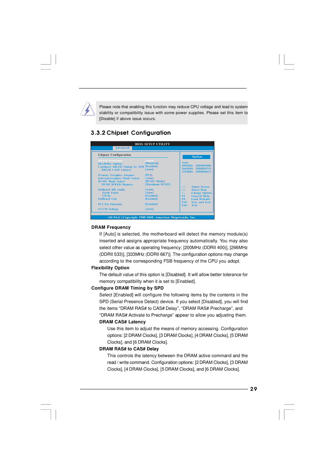
3.3.2 Chipset Configuration
BIOS SETUP UTILITY
Advanced |
|
|
|
| |
Chipset Configuration |
|
| Options | ||
|
|
| |||
DRAM Frequency | [Auto] | Auto |
|
| |
Flexibility Option | [Disabled] |
|
| ||
200MHz | (DDRII400) | ||||
Configure DRAM Timing by SPD [Enabled] | |||||
266MHz | (DDRII533) | ||||
DRAM CAS# Latency | [Auto] | ||||
333MHz | (DDRII667) | ||||
|
| ||||
Primary Graphics Adapter | [PCI] |
|
|
| |
Internal Graphics Mode Select | [Auto] |
|
|
| |
DVMT Mode Select | [DVMT Mode] |
|
|
| |
DVMT/FIXED Memory | [Maximum DVMT] |
| Select Screen | ||
|
|
| |||
OnBoard HD Audio | [Auto] |
| Select Item | ||
Front Panel | [Auto] | + - | Change Option | ||
[Enabled] | F1 | General Help | |||
OnBoard Lan | [Enabled] | F9 | Load Defaults | ||
PCI Fix Function | [Enabled] | F10 | Save and Exit | ||
ESC | Exit | ||||
|
| ||||
VCCM Voltage | [Auto] |
|
|
| |
v02.54 (C) Copyright
DRAM Frequency
If [Auto] is selected, the motherboard will detect the memory module(s) inserted and assigns appropriate frequency automatically. You may also select other value as operating frequency: [200MHz (DDRII 400)], [266MHz (DDRII 533)], [333MHz (DDRII 667)]. The configuration options may change according to the corresponding FSB frequency of the CPU you adopt.
Flexibility Option
The default value of this option is [Disabled]. It will allow better tolerance for memory compatibility when it is set to [Enabled].
Configure DRAM Timing by SPD
Select [Enabled] will configure the following items by the contents in the SPD (Serial Presence Detect) device. If you select [Disabled], you will find the items “DRAM RAS# to CAS# Delay”, “DRAM RAS# Precharge”, and “DRAM RAS# Activate to Precharge” appear to allow you adjusting them.
DRAM CAS# Latency
Use this item to adjust the means of memory accessing. Configuration options: [2 DRAM Clocks], [3 DRAM Clocks], [4 DRAM Clocks], [5 DRAM Clocks], and [6 DRAM Clocks].
DRAM RAS# to CAS# Delay
This controls the latency between the DRAM active command and the read / write command. Configuration options: [2 DRAM Clocks], [3 DRAM Clocks], [4 DRAM Clocks], [5 DRAM Clocks], and [6 DRAM Clocks].
2 9
