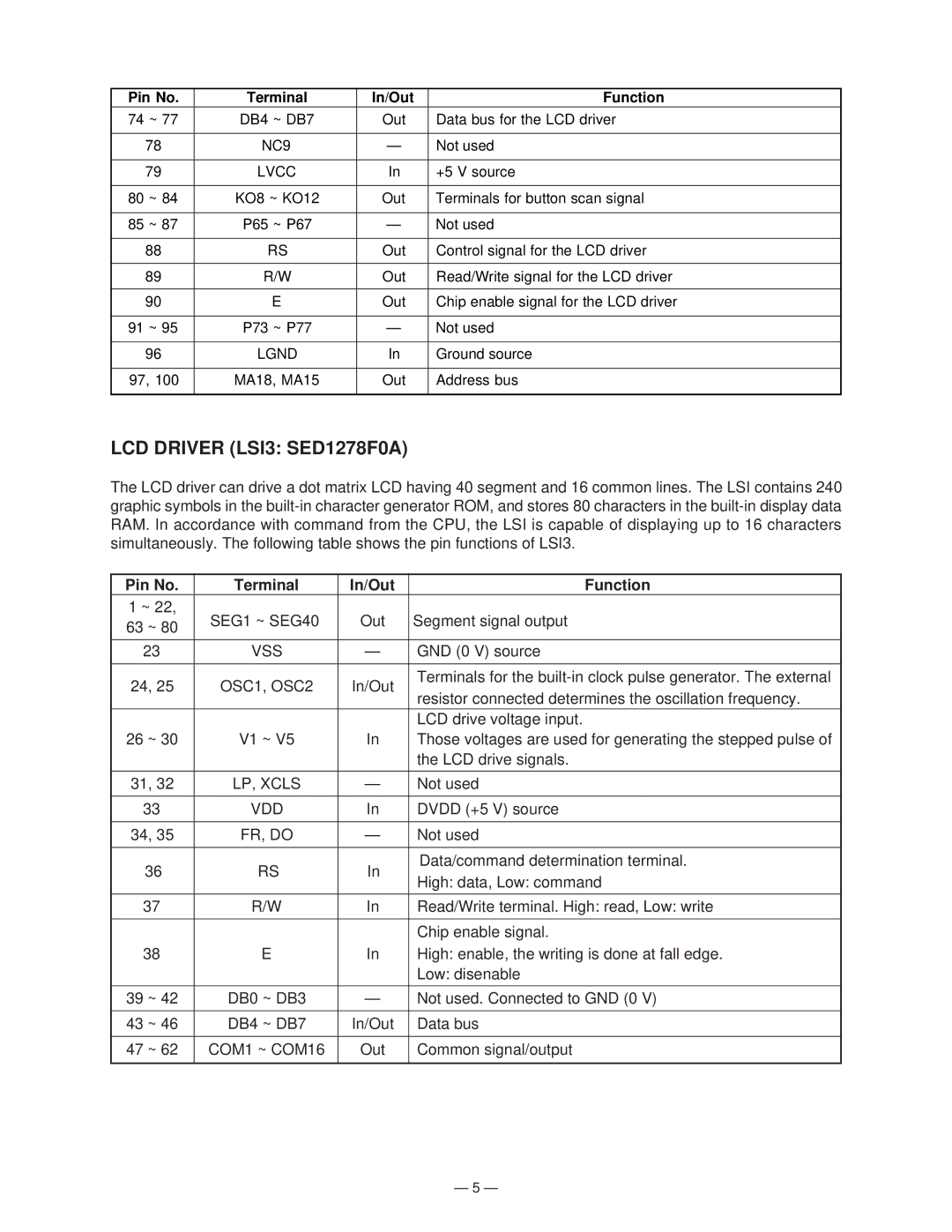
Pin No. | Terminal | In/Out | Function |
74 ~ 77 | DB4 ~ DB7 | Out | Data bus for the LCD driver |
|
|
|
|
78 | NC9 | — | Not used |
|
|
|
|
79 | LVCC | In | +5 V source |
|
|
|
|
80 ~ 84 | KO8 ~ KO12 | Out | Terminals for button scan signal |
|
|
|
|
85 ~ 87 | P65 ~ P67 | — | Not used |
|
|
|
|
88 | RS | Out | Control signal for the LCD driver |
|
|
|
|
89 | R/W | Out | Read/Write signal for the LCD driver |
|
|
|
|
90 | E | Out | Chip enable signal for the LCD driver |
|
|
|
|
91 ~ 95 | P73 ~ P77 | — | Not used |
|
|
|
|
96 | LGND | In | Ground source |
|
|
|
|
97, 100 | MA18, MA15 | Out | Address bus |
|
|
|
|
LCD DRIVER (LSI3: SED1278F0A)
The LCD driver can drive a dot matrix LCD having 40 segment and 16 common lines. The LSI contains 240 graphic symbols in the
Pin No. | Terminal | In/Out | Function | |
1 ~ 22, | SEG1 ~ SEG40 | Out | Segment signal output | |
63 ~ 80 | ||||
|
|
| ||
|
|
|
| |
23 | VSS | — | GND (0 V) source | |
|
|
|
| |
24, 25 | OSC1, OSC2 | In/Out | Terminals for the | |
resistor connected determines the oscillation frequency. | ||||
|
|
| ||
|
|
| LCD drive voltage input. | |
26 ~ 30 | V1 ~ V5 | In | Those voltages are used for generating the stepped pulse of | |
|
|
| the LCD drive signals. | |
|
|
|
| |
31, 32 | LP, XCLS | — | Not used | |
|
|
|
| |
33 | VDD | In | DVDD (+5 V) source | |
|
|
|
| |
34, 35 | FR, DO | — | Not used | |
|
|
|
| |
36 | RS | In | Data/command determination terminal. | |
High: data, Low: command | ||||
|
|
| ||
|
|
|
| |
37 | R/W | In | Read/Write terminal. High: read, Low: write | |
|
|
|
| |
|
|
| Chip enable signal. | |
38 | E | In | High: enable, the writing is done at fall edge. | |
|
|
| Low: disenable | |
|
|
|
| |
39 ~ 42 | DB0 ~ DB3 | — | Not used. Connected to GND (0 V) | |
|
|
|
| |
43 ~ 46 | DB4 ~ DB7 | In/Out | Data bus | |
|
|
|
| |
47 ~ 62 | COM1 ~ COM16 | Out | Common signal/output | |
|
|
|
|
— 5 —
