Schematic Diagrams

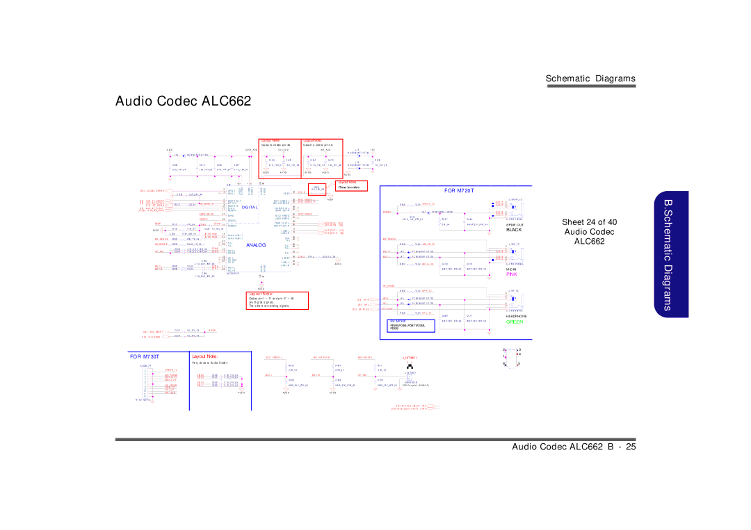
Audio Codec ALC662


Layout Note:

p in

25


Layout Note:

pi n 3 8


Clo se


to

co dec


C los e t o

cod ec


3 . 3V S


3. 3 V S _ A UD


5 V S _A U D


5V S _ A U D


L 4 5

5 V S


L 38


HC B 10 0 5 K F -12 1 T2 0


H CB 1 00 5 K F -1 21 T 20


C 2 5 9


C 5 75


C 56 7


C5 7 0


L 1 6


C 5 76


C 5 06


C5 1 4


C2 36


C 23 7


0. 1 U _1 6 V _0 4

1 0 U _ 1 0V _ 0 8


0 . 1 U _ 1 6V _ 0 4

1 0U _ 10 V _ 08

H CB 1 60 8 K F -1 21 T 25

1 U _1 0 V _0 6


0. 1 U _ 1 6 V _0 4


1 0U _1 0 V _0 8

0. 1 U _ 1 6V _0 4

0 . 1 U _ 1 6V _ 0 4


A UDG


A U DG


A U DG

A UD G


A U DG


U 25


4 7

1 9


2 5 38


Layout

Note:


2


1 0 U _ 1 0V _ 0 8


Close to codec


C 5 30

2 2 P _5 0 V _ 04


3

GP IO 1

SSVD1 SSVD2

DDVD1 DDVD2


DDVA1 DDVA2


V R E F

27

Z 2 4 1 2

C5 6 6


FOR

M720T


[ 2 5 ] C O D E C _E A P D #


GP IO 0


[1 3]

A UD _A Z _ S DO UT


5

S DA T A -OU T


MIC1 -V RE F O -L

28

M IC1 -V RE F O -L


A U D G


Z 2 4 2 4

5

J _ S P DIF _ 7 2


6


32

M I C 1 -V R E F O -R


[1 3]

A UD _A Z _ B IT CL K

R 3 1 2


3 3 _0 4

A Z _ S DIN0 _ R


8

B IT -CL K


MIC 1-V R E F O-R


R 38 5

*0 _0 4

S P DIF O _7 3


Z 2 4 2 5

4


[ 1 3 ] A Z _ S D I N 0


S DA T A -IN

DIG ITA L


R


[1 3]


1 0


S U RR -O UT -L

39


3


A UD _A Z _ S Y N C


S Y N C


[1 3 ,25 ]

A UD _ A Z _ RS T #


1 1

RE S E T #


S URR -OUT -R

41


S P DIF O


L5 4

F C M1 0 05 K F -1 02 T 02


Z 2 4 2 6

2


E A P D _ MO DE


4 7

E A P D


M IC2 -V RE F O

30

M IC2 -V RE F O


Z 2 4 2 7

6

L


31


C 5 7 4


1


S P DIF O


4 8

S P DIF O


L INE 2 -V RE F O

35


0. 0 1 U _ 1 6V _ X 7R _0 4


R 3 3 7


C5 8 0

C1 2 10 3 -1 06 0 9-L


B E E P


Z 2 4 04


F RON T-O UT -L


F R ON T-L

[2 5 ]


R1 17


4 7K _ 0 4

Z 2 40 3

1 2


36


2 20 _ 04


10 0 0 P _5 0 V _X 7 R _ 0 4

SPDIF OUT


P CB E E P


F RO NT -OUT -R


F R ON T-R

[2 5]


A UDG

R1 16


4 . 7K _ 0 4

C5 23

1 U _ 10 V _ 06


L INE 2 -L

14


H P _O UT -L

[2 5]


BLACK


C 23 8

1 0 0P _ 5 0V _ 0 4

JD _S E NS E 1

1 3


15


S e ns e

A (JD

1 )


L INE 2 -R


H P _O UT -R

[25 ]


JD _S E NS E 2

3 4


43


MIC _S E N S E

R3 23


2 0K _ 1 % _0 4

S e ns e

B (JD 2 )


CE N


MIC _ S E NS E


3 7


44


N . C .


ANALOG


L F E


HP _ S E NS E

R3 20


3 9. 2 K _ 1 %_ 0 4


2 9


45


R 38 6

*0 _0 4

MIC 1-R _7 3


J _ MIC _7 2


N . C .


N . C .

46


5


N . C .


C5 5 6


4 . 7U _6 . 3 V _ X5 R _ 0 6

Z 2 40 8

1 6

MIC 2-L


4

R


I N T _ MI C

C5 6 0


4 . 7U _6 . 3 V _ X5 R _ 0 6

Z 2 40 9

1 7


33


MIC1 -R

L 4 8

F C M1 00 5 K F -1 21 T 03


Z 2 4 2 8

3


MIC 2-R


N . C .


1 8

CD -L


J DR E F

40

Z 2 4 2 1

R1 4 2

2 0 K _1 % _ 04


MIC1 -L

L 4 7

F C M1 00 5 K F -1 21 T 03


Z 2 4 2 9

2

L


C 56 3


1 9


23


Z 2 4 3 0 6


2 0

CD -GND


L INE 1 -L


1


4 . 7 U _ 6. 3 V _ X5 R _0 6


CD -R


24


A U D G


R 38 7

*0 _0 4 MI C 1-L _ 73

C5 7 8


C5 7 9

C1 2 10 3 -D0 6 09 -L


MI C 1-L

R3 29


2 1


1 2


L INE 1 -R


1 K _0 4


Z 2 41 0

MIC 1-L


S S S S


MIC 1-R

R3 30


1 K _0 4


Z 2 41 1

2 2


6 80 P _ 50 V _ X 7R _0 4

68 0 P _ 50 V _ X7 R _ 0 4

MIC IN


MIC 1-R


AV AV


C 56 5


A L C6 6 2-G R


2 6 42


PINK


4 . 7 U _ 6. 3 V _ X5 R

_0 6


HP _ S E NS E


A UD G


R 38 8

*0 _0 4 HP -R _7 3


J _ HP _ 7 2


Lay ou t N ot e:


5


47

~

48


4


Cod ec

pi n 1


~

11

an d p in


[ 2 5]

H P -R

HP -R

L 4 6

F C M1 00 5 K F -1 21 T 03


3

R


are

D igi tal


s ign als .


[25 ]

HP -L

HP -L

L 5 0

F C M1 00 5 K F -1 21 T 03


2


The

o the rs

ar e a nal og

si gna ls.


6

L


[2 5 ] HP _ P L UG

H P _P L UG


1


R 38 9

*0 _0 4 H P -L _ 73


C1 2 10 3 -6 06 0 9-L


For

M730T


C 5 8 8


C5 7 7

HEADPHONE


6 80 P _ 50 V _ X 7R _0 4

68 0 P _ 50 V _ X7 R _ 0 4

GREEN


R385,R386,R387,R388,


[2 6 ] K B C _B E E P

C2 2 7


1 U _ 10 V _ 0 6

B E E P


R389


[1 5 ]

IC H _ S P K R

C2 2 8


1 U _ 10 V _ 0 6


2


3

FOR

M730T


Layout

Note:


M IC1 -V RE F O -L


MIC 1-V R E F O-R


MIC2 -V R E F O


J_I NT MIC 1


1


4


C ode c


5


J_ A UD _7 3


Ve ry

clo se

to

Au dio


R3 3 3


R 33 4


R7 2

2

1


6


1

S P DIF O_ 7 3


2 . 2K _ 0 4


2 . 2 K _0 4


4 . 7K _ 0 4


2


J _I N T MI C 1


3

MI C _ S E N S E


Z 24 0 8

C5 4 8

0. 1U _1 6 V _0 4


MIC1 -L


MIC 1 -R


INT _ MIC


1


4

MIC1 -R _ 7 3


Z 24 0 9

C5 5 5

0. 1U _1 6 V _0 4


5

MIC1 -L _7 3


C 5 6 8


C 56 9


C1 5 5


2


6


Z 24 1 0

C5 5 8

0. 1U _1 6 V _0 4


8 82 6 6 -02 0 01


7

HP _ S E NS E


Z 24 1 1

C5 6 2

0. 1U _1 6 V _0 4


6 80 P _ 50 V _ X7 R _0 4


6 8 0P _ 5 0V _ X 7 R _ 04


6 80 P _ 50 V _ X7 R _0 4

P CB F o o tpri n t = 8 8 26 6 -2 L


8


H P -R _ 7 3


9

HP -L _7 3


10

HP _ P LU G


A UD G


A UD G


A U D G


11


12


*8 7 15 1 -12 0 71 G


[ 12 , 1 3, 1 6 , 19 , 2 1 , 25 , 2 7]


5V S


[5 ,8.. 1 6 ,18 .. 2 3,2 5 .. 2 7,3 1 ]

3 . 3V S


Sheet 24 of 40

Audio Codec

ALC662

B.Schematic Diagrams

Audio Codec ALC662 B - 25

Page 99
Image 99
Clevo M730T, M729T, M728T manual Sheet 24 Audio Codec ALC662

M728T, M729T, M730T specifications

The Clevo M730T, M729T, and M728T series are a trio of gaming laptops that showcase the brand's commitment to delivering high-performance portable computing solutions. Each of these models carries unique features, technologies, and characteristics that cater to a variety of user needs, from gaming enthusiasts to professional content creators.

Starting with the Clevo M730T, this model is designed for gamers who demand power and efficiency. It comes equipped with the latest Intel Core processors, providing superior performance for demanding applications and smooth gaming experiences. The NVIDIA GeForce graphics card enhances visual capabilities, allowing users to enjoy high settings in modern games. One of the standout features of the M730T is its vibrant Full HD display, which offers rich colors and excellent viewing angles, ensuring an immersive visual experience.

Moving on to the Clevo M729T, this model is a slightly upgraded version, incorporating advanced thermal management systems to keep the laptop cool during extended gaming sessions. This feature is crucial for maintaining performance and prolonging the lifespan of the internal components. Like the M730T, it supports high-performance graphics and boasts an impressive resolution, but its enhanced cooling technology sets it apart. The M729T also emphasizes connectivity, featuring a variety of ports including USB-C, HDMI, and Ethernet, which cater to gamers looking for extensive peripheral support.

Finally, the Clevo M728T model offers a balance of performance and portability. Its lighter design and slim profile make it an appealing choice for users who need a powerful laptop that is easy to carry. Despite its compact form, the M728T still packs a punch with its capable hardware configuration, including efficient battery life that allows for extended usage without being tethered to power outlets. Its keyboard is built for comfort, featuring customizable backlighting options that enhance the gaming experience in low-light environments.

In summary, the Clevo M730T, M729T, and M728T models each bring their own unique set of features and technologies to the table. From powerful processing capabilities and advanced graphics to superior cooling and portability, these laptops are well-suited for gamers and professionals alike. As technology continues to advance, these models represent a solid choice for those seeking a reliable and high-performing laptop.