CY62147DV18
MoBL2™
4-Mb (256K x 16) Static RAM
Features
•Very high speed: 55 ns and 70 ns
•Wide voltage range: 1.65V – 2.25V
•
•
—Typical active current: 1 mA @ f = 1 MHz
—Typical active current: 6 mA @ f = fmax
•Ultra low standby power
•Easy memory expansion with CE, and OE features
•Automatic
•CMOS for optimum speed/power
•Packages offered
Functional Description[1]
The CY62147DV18 is a
mode reducing power consumption by more than 99% when deselected (CE HIGH or both BLE and BHE are HIGH). The input/output pins (I/O0 through I/O15) are placed in a
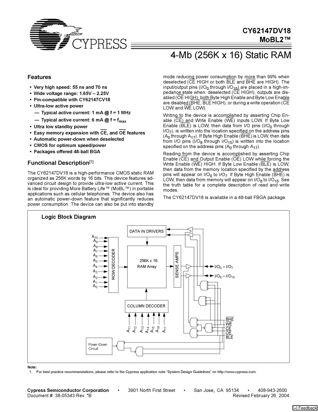
Writing to the device is accomplished by asserting Chip En- able (CE) and Write Enable (WE) inputs LOW. If Byte Low Enable (BLE) is LOW, then data from I/O pins (I/O0 through I/O7), is written into the location specified on the address pins (A0 through A17). If Byte High Enable (BHE) is LOW, then data from I/O pins (I/O8 through I/O15) is written into the location specified on the address pins (A0 through A17).
Reading from the device is accomplished by asserting Chip Enable (CE) and Output Enable (OE) LOW while forcing the Write Enable (WE) HIGH. If Byte Low Enable (BLE) is LOW, then data from the memory location specified by the address pins will appear on I/O0 to I/O7. If Byte High Enable (BHE) is LOW, then data from memory will appear on I/O8 to I/O15. See the truth table for a complete description of read and write modes.
The CY62147DV18 is available in a
Logic Block Diagram
A10
A9 ![]()
![]()
DATA IN DRIVERS ![]()
![]()
![]()
![]()
A8 |
|
| DECODER | ||
|
| ||||
A7 |
| ||||
| |||||
A4 |
| ||||
A6 |
|
| |||
A5 |
|
| |||
A3 |
|
|
| ROW | |
|
|
| |||
A2 |
|
|
| ||
|
|
| |||
A1 |
|
| |||
|
| ||||
A0 |
|
| |||
|
| ||||
256K x 16 RAM Array
![]()
![]()
![]()
![]() SENSE AMPS
SENSE AMPS
![]()
![]()
![]()
![]() I/O0 – I/O7
I/O0 – I/O7
![]()
![]()
![]()
![]() I/O8 – I/O15
I/O8 – I/O15
Power
COLUMN DECODER |
| ||||||
|
|
|
|
|
|
| BHE |
11 | 12 | 13 | 14 | 15 | 16 | 17 | WE |
CE | |||||||
A | A | A | A A A | A | OE | ||
|
|
|
|
|
|
| |
|
|
|
|
|
|
| BLE |
Note:
1.For best practice recommendations, please refer to the Cypress application note “System Design Guidelines” on http://www.cypress.com.
Cypress Semiconductor Corporation | • | 3901 North First Street | • | San Jose, CA 95134 | • | |
Document #: |
|
|
| Revised February 26, 2004 | ||
[+] Feedback