CY62147EV30 specifications
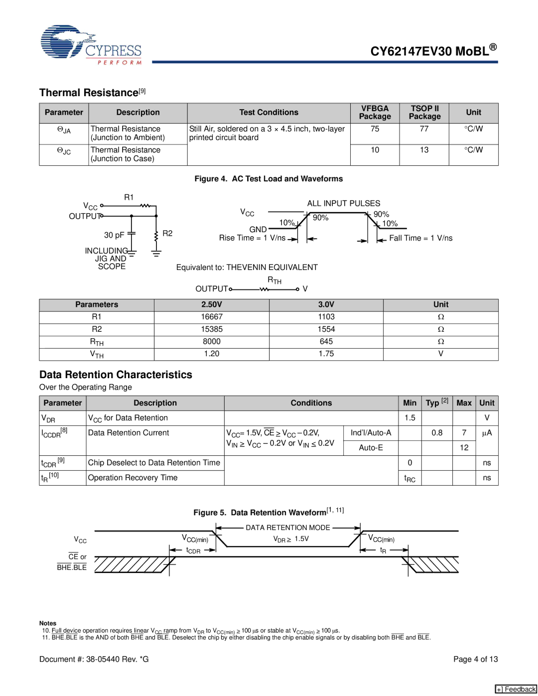
The Cypress CY62147EV30 is a high-performance, low-power Static Random Access Memory (SRAM) device that has garnered attention in various applications due to its remarkable features and technologies. This SRAM provides a robust solution for applications requiring fast, reliable data access in a compact form factor.One of the main features of the CY62147EV30 is its density of 1 Megabit, which is organized as 128K x 8 bits. This configuration allows for significant data storage while maintaining a small footprint, making it suitable for embedded systems and portable devices. The device operates with a voltage range of 2.7V to 3.6V, which is critical for battery-operated applications where power consumption is a key concern.
The CY62147EV30 utilizes a synchronous operation mode, which contributes to faster data transfer rates. With access times as low as 30 nanoseconds, it provides swift read and write operations, enabling quick response times in demanding computational environments. This speed is particularly beneficial for applications in telecommunications, automotive systems, and consumer electronics, where real-time data processing is essential.
Another notable characteristic of the CY62147EV30 is its low power consumption. It offers significantly reduced active and standby current levels, which is vital for extending the battery life of portable devices. The device employs advanced power management features that help optimize performance while consuming minimal energy.
Additionally, the CY62147EV30 includes a variety of features designed to enhance reliability and data integrity. These include an automatic power-down feature that reduces power usage during inactive periods and built-in write protection to safeguard against unintended data corruption. The device also adheres to strict quality and reliability standards, making it a trustworthy choice for mission-critical applications.
In summary, the Cypress CY62147EV30 is distinguished by its 1 Megabit density, low power consumption, fast access times, and enhanced reliability features. These characteristics make it an ideal solution for a wide range of applications, from automotive systems to portable devices, where performance, efficiency, and reliability are paramount. With its advanced technological design, the CY62147EV30 continues to meet the evolving demands of modern electronic applications.

