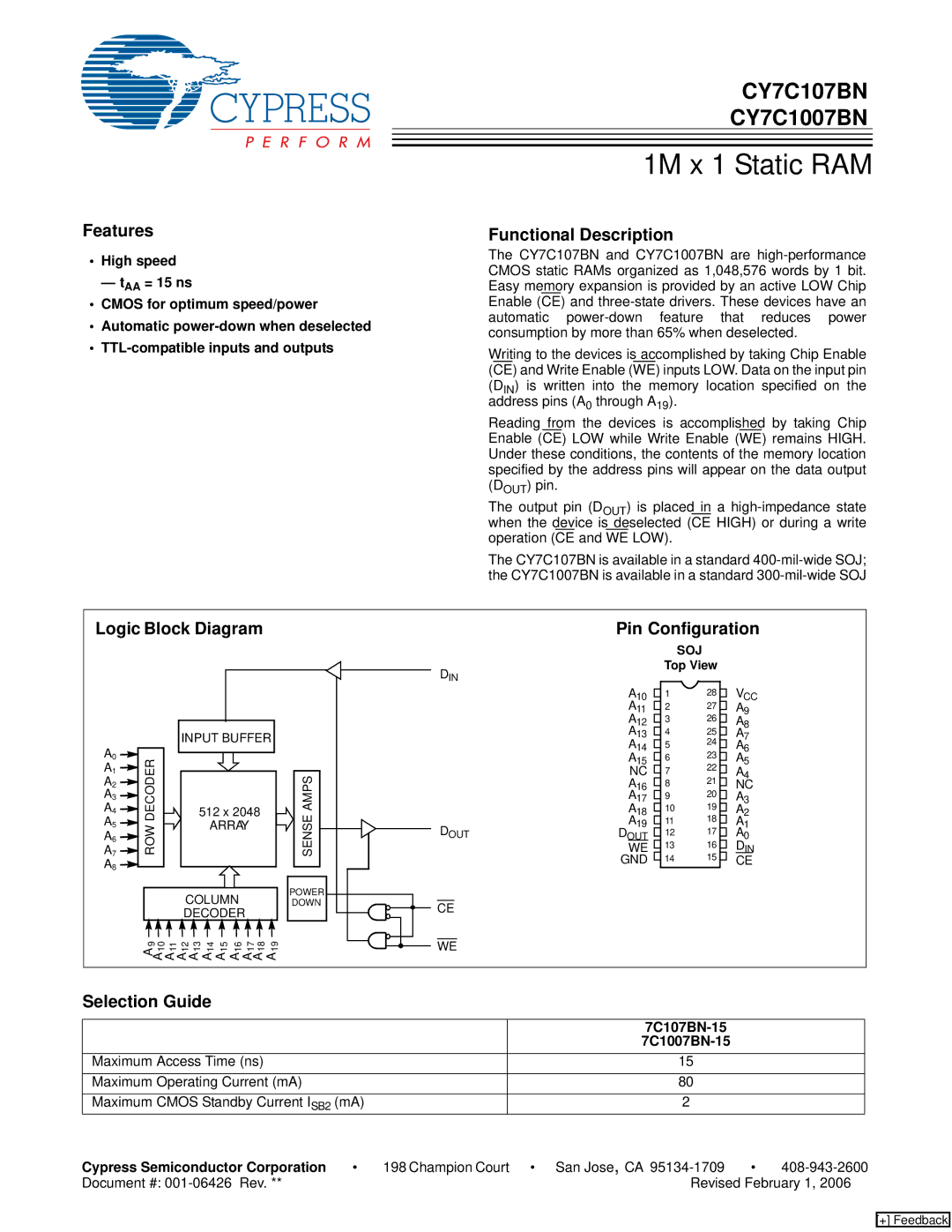
CY7C107BN, CY7C1007BN specifications
The Cypress CY7C107BN and CY7C1007BN are versatile synchronous static RAM (SRAM) devices that are widely used in various electronic applications, including networking, telecommunications, and consumer electronics. These devices are designed to meet the demands for high-speed memory accesses while providing low power consumption and high reliability, making them an ideal choice for designers seeking efficient memory solutions.One of the main features of the CY7C107BN and CY7C1007BN is their high-speed access time. Both chips offer access times as fast as 10 nanoseconds, which allows devices using these memories to process data at impressive rates. This speed is particularly beneficial for applications requiring rapid read and write operations, such as cache memory or data buffering in high-performance computing environments.
In terms of memory density, the CY7C107BN offers a capacity of 1 Megabit, while the CY7C1007BN provides a greater capacity of 2 Megabits. This makes both chips suitable for varying storage requirements, allowing designers to select the appropriate size based on their application's memory needs. The memory architecture of these SRAMs consists of a static cell design, which ensures data retention without the need for refresh cycles, contrasting with dynamic RAM (DRAM) technologies. This characteristic not only simplifies system design but enhances performance and reliability.
The Cypress SRAMs are implemented in a single 5-volt power supply range, facilitating compatibility with a wide range of existing systems. Their low standby current consumption is another notable advantage, enabling battery-operated devices to operate for extended periods without significant power drain.
Moreover, the CY7C107BN and CY7C1007BN incorporate advanced CMOS technology, which contributes to their low power dissipation and high noise immunity. Designers appreciate the integration and ease of implementation made possible by 10 leading-edge package options available for these devices.
Additionally, both memory chips support common SRAM functionalities, including asynchronous read and write controls, enabling straightforward interfacing with microcontrollers and digital signal processors. With built-in features for write enable, output enable, and chip select, these SRAMs facilitate flexible memory management and control in diverse applications.
In summary, the Cypress CY7C107BN and CY7C1007BN SRAMs represent robust and efficient memory solutions that offer high speeds, low power consumption, and significant reliability. Their features make them suitable for a wide range of electronic applications, solidifying their position as trusted components in the evolving landscape of semiconductor technologies.

