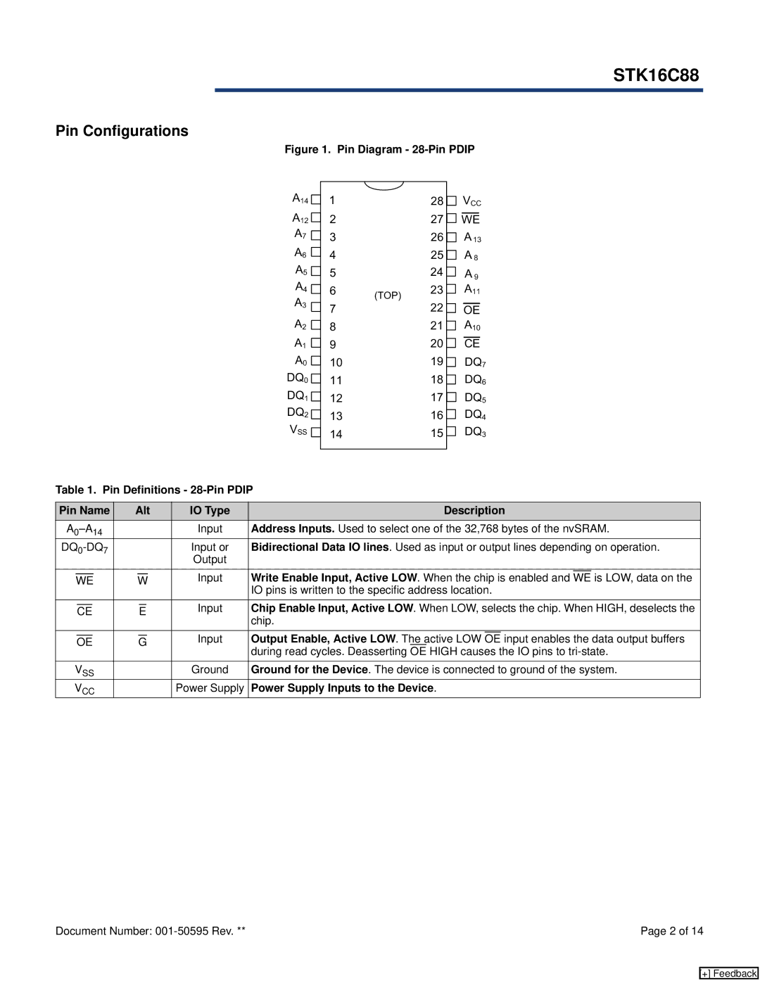
STK16C88 specifications
The Cypress STK16C88 is a highly regarded SRAM (Static Random Access Memory) device that is designed for high-performance computing applications. As a member of the Cypress family of memory solutions, the STK16C88 is known for its efficiency, speed, and reliability, making it a popular choice among engineers and developers seeking robust memory solutions for their projects.One of the key features of the STK16C88 is its high-speed access capability. It operates at a maximum access time of just 55 nanoseconds, enabling rapid data retrieval and processing. This characteristic makes it particularly suitable for applications requiring quick response times, such as telecommunications, networking equipment, and industrial automation systems.
The STK16C88 boasts a dual-port architecture, which allows simultaneous access to data from multiple devices. This enhances the flexibility of the memory chip, making it ideal for multi-processor systems where efficient data sharing is critical. The dual-port feature also facilitates easier designs for applications that require real-time data processing and eliminates potential bottlenecks that might hinder system performance.
In terms of capacity, the STK16C88 provides 128K bits of memory, organized as 16K x 8 bits. This allocation of memory provides ample space for storing data and program code, making it versatile for various applications, including embedded systems and consumer electronics. Additionally, it supports asynchronous read/write operations, ensuring that the system can perform tasks without being held up by the memory component.
Another important characteristic of the STK16C88 is its low power consumption, which is vital for battery-operated devices and portable electronics. The device operates with a supply voltage of 3.3V, making it suitable for modern low-power applications. Its energy-efficient design extends battery life and reduces heat generation, further enhancing the reliability of the systems that utilize it.
Moreover, the STK16C88 is characterized by its compatibility with various industry-standard memory interfaces, allowing for seamless integration into existing systems. The simplicity of implementation, combined with its robust performance and reliability, makes it an excellent choice for manufacturers looking to enhance the capabilities of their devices.
In conclusion, the Cypress STK16C88 is a high-performance, low-power SRAM solution that is well-suited for various applications ranging from telecommunications to consumer electronics. Its key features, including dual-port architecture, high-speed access, and low power consumption, position it as a valuable component in the design of contemporary electronic systems.

