ST92195B - GENERAL INFORMATION
PIN DESCRIPTION (Cont’d)
RESET Reset (input, active low). The ST9+ is ini- tialised by the Reset signal. With the deactivation of RESET, program execution begins from the Program memory location pointed to by the vector contained in program memory locations 00h and 01h.
R/G/B Red/Green/Blue. Video color analog DAC outputs.
FB Fast Blanking. Video analog DAC output.
VDD Main power supply voltage (5V10%, digital)
WSCF, WSCR Analog pins for the VPS/WSS slic- er line PLL (See note 1).
MCFM Analog pin for the display pixel frequency multiplier.
OSCIN, OSCOUT Oscillator (input and output). These pins connect a
VSYNC Vertical Sync. Vertical video synchronisa- tion input to OSD. Positive or negative polarity.
HSYNC/CSYNC Horizontal/Composite sync. Hori- zontal or composite video synchronisation input to OSD. Positive or negative polarity.
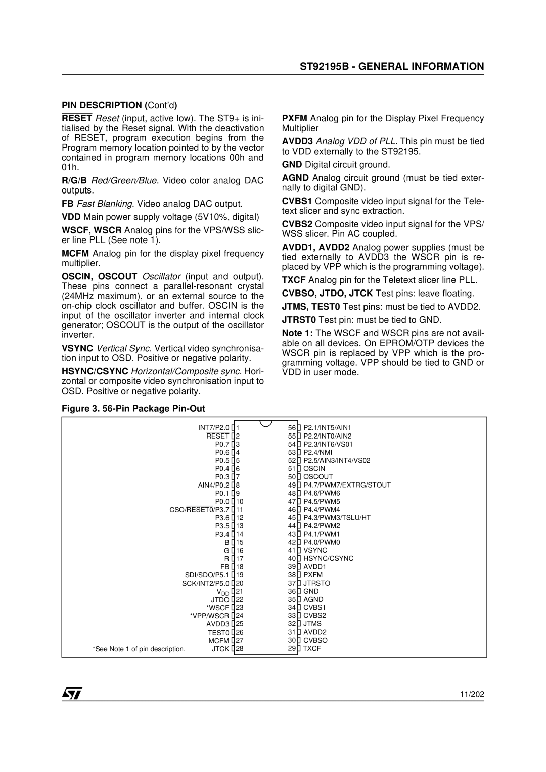
Figure 3. 56-Pin Package Pin-Out
PXFM Analog pin for the Display Pixel Frequency Multiplier
AVDD3 Analog VDD of PLL. This pin must be tied to VDD externally to the ST92195.
GND Digital circuit ground.
AGND Analog circuit ground (must be tied exter- nally to digital GND).
CVBS1 Composite video input signal for the Tele- text slicer and sync extraction.
CVBS2 Composite video input signal for the VPS/ WSS slicer. Pin AC coupled.
AVDD1, AVDD2 Analog power supplies (must be tied externally to AVDD3 the WSCR pin is re- placed by VPP which is the programming voltage).
TXCF Analog pin for the Teletext slicer line PLL.
CVBSO, JTDO, JTCK Test pins: leave floating.
JTMS, TEST0 Test pins: must be tied to AVDD2.
JTRST0 Test pin: must be tied to GND.
Note 1: The WSCF and WSCR pins are not avail- able on all devices. On EPROM/OTP devices the WSCR pin is replaced by VPP which is the pro- gramming voltage. VPP should be tied to GND or VDD in user mode.
| INT7/P2.0 |
|
|
|
| P2.1/INT5/AIN1 | |||
|
| 1 | 56 |
| |||||
|
|
| |||||||
|
|
|
|
|
| 2 | 55 |
| P2.2/INT0/AIN2 |
|
| RESET |
|
| |||||
|
|
| P0.7 |
| 3 | 54 |
| P2.3/INT6/VS01 | |
|
|
| |||||||
|
|
| P0.6 |
| 4 | 53 |
| P2.4/NMI | |
|
|
| |||||||
|
|
| P0.5 |
| 5 | 52 |
| P2.5/AIN3/INT4/VS02 | |
|
|
| |||||||
|
|
| P0.4 |
| 6 | 51 |
| OSCIN | |
|
|
| |||||||
|
|
| P0.3 |
| 7 | 50 |
| OSCOUT | |
|
|
| |||||||
| AIN4/P0.2 |
| 8 | 49 |
| P4.7/PWM7/EXTRG/STOUT | |||
|
|
| |||||||
|
|
| P0.1 |
| 9 | 48 |
| P4.6/PWM6 | |
|
|
| |||||||
|
|
| P0.0 |
| 10 | 47 |
| P4.5/PWM5 | |
|
|
| |||||||
|
|
|
| 11 | 46 |
| P4.4/PWM4 | ||
CSO/RESET0/P3.7 |
|
| |||||||
|
|
| P3.6 |
| 12 | 45 |
| P4.3/PWM3/TSLU/HT | |
|
|
| |||||||
|
|
| P3.5 |
| 13 | 44 |
| P4.2/PWM2 | |
|
|
| |||||||
|
|
| P3.4 |
| 14 | 43 |
| P4.1/PWM1 | |
|
|
| |||||||
|
|
| B |
| 15 | 42 |
| P4.0/PWM0 | |
|
|
| |||||||
|
|
| G |
| 16 | 41 |
| VSYNC | |
|
|
| |||||||
|
|
| R |
| 17 | 40 |
| HSYNC/CSYNC | |
|
|
| |||||||
|
|
| FB |
| 18 | 39 |
| AVDD1 | |
|
|
| |||||||
SDI/SDO/P5.1 |
| 19 | 38 |
| PXFM | ||||
|
| ||||||||
SCK/INT2/P5.0 |
| 20 | 37 |
| JTRSTO | ||||
|
| ||||||||
|
|
| VDD |
| 21 | 36 |
| GND | |
|
|
| |||||||
|
|
| |||||||
|
| JTDO |
| 22 | 35 |
| AGND | ||
|
| *WSCF |
| 23 | 34 |
| CVBS1 | ||
|
|
| |||||||
| *VPP/WSCR |
| 24 | 33 |
| CVBS2 | |||
|
|
| |||||||
|
| AVDD3 |
| 25 | 32 |
| JTMS | ||
|
|
| |||||||
|
| TEST0 |
| 26 | 31 |
| AVDD2 | ||
|
|
| |||||||
|
|
| |||||||
|
| MCFM |
| 27 | 30 |
| CVBSO | ||
*See Note 1 of pin description. |
| JTCK |
| 28 | 29 |
| TXCF | ||
|
| ||||||||
|
|
|
|
|
|
|
|
|
|
|
|
|
|
|
|
|
|
|
|
11/202
