USQ Series | 2 0 A , S I N G L E O U T P U T D C / D C C O N V E R T E R S |
|
|
Absolute Maximum Ratings
Input Voltage: | 24V models | 48V models |
Continuous: | 39 Volts | 81 Volts |
Transient (100msec) | 50 Volts | 100 Volts |
Input | Input Current must be <5A. 1 minute | |
| duration. Fusing recommended. | |
Output Current | Current limited. Devices can withstand | |
| an indefinite output short circuit. | |
On/Off Control (Pin 2) Max. Voltages |
|
|
Referenced to |
| |
Storage Temperature |
| |
Lead Temperature (Soldering, 10 sec.) | +300°C |
|
These are stress ratings. Exposure of devices to any of these conditions may adversely affect
T E C H N I C A L N O T E S
Removal of Soldered USQ's from PCB's
Should removal of the USQ from its soldered connection be needed, it is very important to thoroughly
Input Source Impedance
impedance as highly inductive source impedance can affect system stability. In Figure 2, CBUS and LBUS simulate a typical dc voltage bus. Your specific system configuration may necessitate additional considerations.
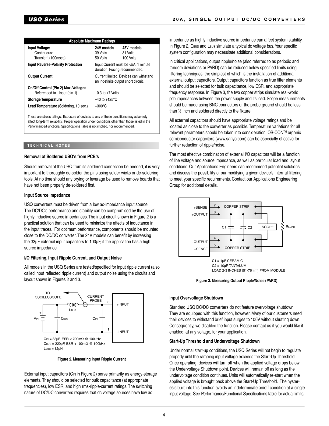
In critical applications, output ripple/noise (also referred to as periodic and random deviations or PARD) can be reduced below specified limits using filtering techniques, the simplest of which is the installation of additional external output capacitors. Output capacitors function as true filter elements and should be selected for bulk capacitance, low ESR, and appropriate frequency response. In Figure 3, the two copper strips simulate
All external capacitors should have appropriate voltage ratings and be located as close to the converter as possible. Temperature variations for all relevant parameters should be taken into consideration.
The most effective combination of external I/O capacitors will be a function of line voltage and source impedance, as well as particular load and layout conditions. Our Applications Engineers can recommend potential solutions and discuss the possibility of our modifying a given device’s internal filtering to meet your specific requirements. Contact our Applications Engineering Group for additional details.
USQ converters must be driven from a low
+SENSE
+OUTPUT
7 | COPPER STRIP |
|
8
C1C2
4
5
COPPER STRIP
SCOPE
RLOAD
I/O Filtering, Input Ripple Current, and Output Noise
All models in the USQ Series are tested/specified for input ripple current (also called input reflected ripple current) and output noise using the circuits and layout shown in Figures 2 and 3.
| TO | CURRENT |
|
|
OSCILLOSCOPE |
|
| ||
|
| PROBE | 3 | +INPUT |
|
|
| ||
|
|
|
| |
| + | LBUS |
|
|
|
|
|
| |
VIN | CBUS | CIN |
|
|
| – |
|
|
|
|
|
| 1 | |
|
|
|
| |
CIN = 33µF, ESR < 700mΩ @ 100kHz
CBUS = 220µF, ESR < 100mΩ @ 100kHz
LBUS = 12µH
Figure 2. Measuring Input Ripple Current
External input capacitors (CIN in Figure 2) serve primarily as
C1 = 1µF CERAMIC
C2 = 10µF TANTALUM
LOAD
Figure 3. Measuring Output Ripple/Noise (PARD)
Input Overvoltage Shutdown
Standard USQ DC/DC converters do not feature overvoltage shutdown. They are equipped with this function, however. Many of our customers need their devices to withstand brief input surges to 100V without shutting down. Consequently, we disabled the function. Please contact us if you would like it enabled, at any voltage, for your application.
Start-Up Threshold and Undervoltage Shutdown
Under normal
4
