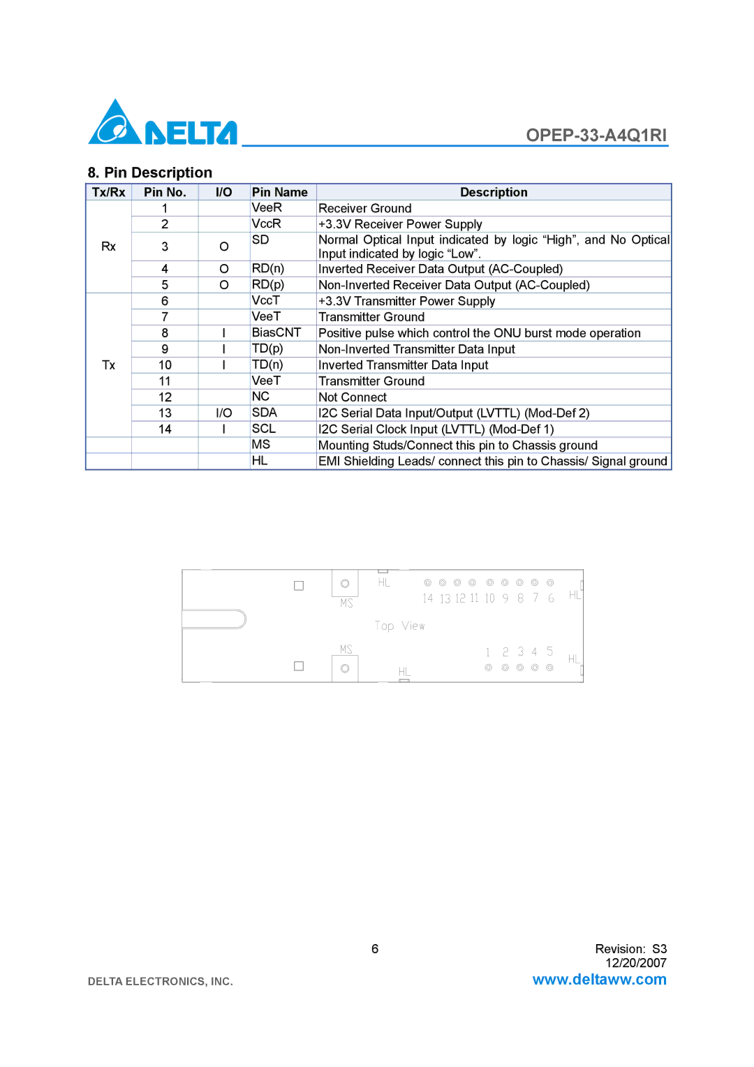
OPEP-33-A4Q1RI specifications
Delta Electronics OPEP-33-A4Q1RI is a high-performance power supply designed to cater to modern electronic applications. This product is part of Delta's extensive range of power solutions, known for their reliability, efficiency, and advanced technologies. The OPEP-33-A4Q1RI stands out for its compact design while providing robust power performance and versatility, making it suitable for various industries, including telecommunications, industrial automation, and medical devices.One of the main features of the OPEP-33-A4Q1RI is its output power capability of 33 watts. This power supply unit (PSU) operates over a wide input voltage range, accommodating both AC and DC input sources. The ability to work within a diverse range of voltage inputs enhances the product's adaptability to different system requirements and geographical power standards, making it ideal for global applications.
In terms of efficiency, the OPEP-33-A4Q1RI boasts a high efficiency rating, which contributes to lower energy consumption and reduced heat generation. This is particularly important for applications requiring continuous operation, as it helps maintain performance stability while minimizing cooling requirements. Supporting energy-saving features helps organizations meet energy efficiency regulations.
The OPEP-33-A4Q1RI is equipped with over-voltage, over-current, and short-circuit protection features. These safety mechanisms ensure reliable operation and protect both the power supply and connected devices from damage. This enhances the overall reliability of applications powered by this unit, which is crucial for mission-critical systems.
Another notable characteristic is its compact form factor, making it easy to integrate into various setups. This design consideration allows for flexibility in applications where space is at a premium. Additionally, the power supply meets international safety and quality standards, assuring users of its dependability and compliance with global requirements.
Overall, Delta Electronics OPEP-33-A4Q1RI represents a synthesis of high performance, efficiency, and safety in a compact format. Its features and robust design make it an excellent choice for developers and engineers looking for reliable power solutions for their electronic systems. With Delta Electronics' reputation for quality and innovation, the OPEP-33-A4Q1RI is a formidable option in the competitive landscape of power supplies.

