|
|
|
|
| |||
6. Pin Description |
|
|
|
| |||
Tx/Rx | Pin No. | I/O | Pin Name | Description | |||
| 1 |
| VeeR | Receiver Ground | |||
| 2 |
| VccR | +3.3V Receiver Power Supply | |||
Rx | 3 | O | SD | Normal Optical Input indicated by logic “High”, and No Optical | |||
|
| Input indicated by logic “Low”. | |||||
|
|
|
|
| |||
| 4 | O | RD(n) | Inverted Receiver Data Output | |||
| 5 | O | RD(p) | ||||
| 6 |
| VccT | +3.3V Transmitter Power Supply | |||
| 7 |
| VeeT | Transmitter Ground | |||
Tx | 8 | I | Tx_Dis | LVTTL Logic “High” or “Open” to Disable Transmitter, and Enable | |||
Transmitter by Logic “Low”. | |||||||
|
|
|
|
| |||
| 9 | I | TD(p) | ||||
| 10 | I | TD(n) | Inverted Transmitter Data Input | |||
|
|
| MS | Mounting studs/ connect this pin to Chassis ground | |||
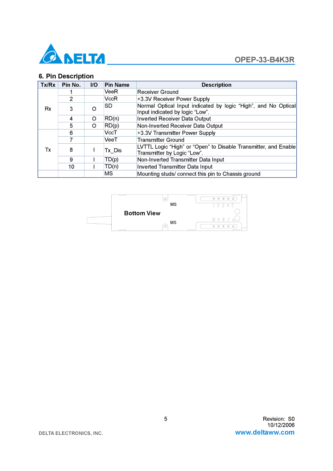
MS
Bottom View
MS
5 | Revision: S0 |
| 10/12/2006 |
DELTA ELECTRONICS, INC. | www.deltaww.com |