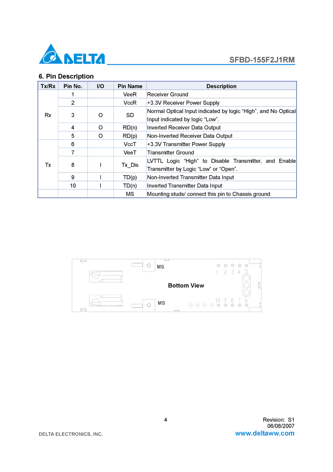
SFBD-155F2J1RM specifications
Delta Electronics SFBD-155F2J1RM is a cutting-edge power supply unit known for its efficient power conversion and robust design tailored for critical industrial applications. This model stands out in the market for its impressive performance specifications, making it suitable for a variety of demanding environments, including telecommunications, data centers, and industrial machinery.One of the defining features of the SFBD-155F2J1RM is its high efficiency rating, often exceeding 94%. This superior efficiency minimizes energy loss, which translates to lower operational costs and reduced heat emissions, thereby enhancing the reliability of connected equipment. The power supply is designed to comply with international energy standards, satisfying both global and local regulations.
The unit boasts a robust output current capability, providing stable and reliable power up to 155W. Its output voltage can be easily adjusted, catering to diverse applications while ensuring a stable supply across varying loads. The SFBD-155F2J1RM also includes comprehensive protection features such as over-voltage, over-current, and thermal protection, safeguarding both the power supply and connected devices from potential damage.
Equipped with a wide input voltage range, the SFBD-155F2J1RM is versatile enough to operate in different geographical locations, accommodating the varying voltage levels prevalent in various regions. Its compact design not only optimizes space in installations but also allows for easy integration into existing systems.
The power supply utilizes advanced switching technologies, ensuring rapid response times and consistent performance under load changes. This technology enhances the overall reliability of the unit, reducing downtime and maintenance needs, which is crucial for mission-critical applications.
In terms of connectivity, the SFBD-155F2J1RM features standard connectors compatible with various industry applications, promoting easy installation and replacement. Additionally, it supports remote monitoring, allowing users to track performance metrics and receive alerts for potential issues.
In summary, Delta Electronics SFBD-155F2J1RM is a robust, high-efficiency power supply unit engineered for the demands of modern industrial applications. Its advanced features, coupled with safety protections and versatile operational capabilities, make it a preferred choice among professionals seeking reliable power solutions.

