LBI-31629
Q202. The RF power output from Pin 2 of the
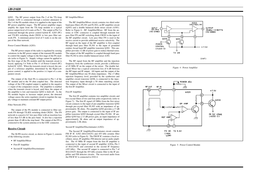
Power Control Module (A203):
The RF power output of the radio is regulated by sensing variations in the RF power output of the transmit PA module to control the supply voltage to the first stage of the PA mod- ule (refer to Figure 5). Supply voltage cannot be applied to the first stage of the PA module until the transmit circuit is keyed, applying 5.4 Volts to Pin 11 of Power Control (PC) hybrid IC A203. When the transmit circuit is keyed, the out- put of a reference amplifier, determined by the
The output of the final PA is connected to Pin 1 of the PC module and to the 50 ohm coupled line. The detected voltage of the CM coupled output is applied to the negative
Filter Network (FN):
The output of the PA module is connected to filter net- work FN through
Receive Circuit
The
∙RF Amplifier/Mixer
∙First IF Amplifier
∙Second IF Amplifier/Discriminator
RF Amplifier/Mixer:
The RF Amplifier/Mixer circuit contains two third order band pass filters (FL301 and FL302), an RF amplifier circuit (Q301) and a double balanced diode mixer circuit (A301). Refer to Figure 6 - RF Amplifier/Mixer. RF from the an- tenna or UDC connector is coupled through transmit low pass filter FN and RF switching diode CR201 to the input of the RF amplifier circuit. Low pass filter FN is used in the receive circuit to provide additional receive selectivity. The RF signal on the input of the RF amplifier is first coupled through band pass filter FL301 to the input of grounded emitter, broad band RF amplifier transistor Q301. This am- plifier provides 12 dB of power gain to reduce thermal noise. The output of the RF amplifier is coupled through band pass filter FL302 to drive double balanced mixer A301.
The RF signal from the RF amplifier and the injection frequency from the synthesizer circuit, provide a difference of 45 MHz IF on the output of the mixer. The double bal- anced Mixer has a typical conversion loss of 6 dB between the RF input and IF output. All inputs and the output of the RF Amplifier/Mixer one 50 ohms impedance. The +7 dBm injection frequency level, provided by the synthesizer and amplifier circuit transistor Q106, is connected to the injec- tion frequency input through a 50 ohms matching circuit. The output of the Mixer circuit is connected to the input of the first IF Amplifier.
First IF Amplifier:
The first IF amplifier contains two amplifier circuits and two crystal filters of two and four poles respectively (refer to Figure 7). The first IF signal (45 MHz) from the first mixer circuit connects to the input of
Second IF Amplifier/Discriminator (A302):
The Second IF Amplifier/Discriminator circuit contains FM IF IC A302 (HA12442V) and 455 kHz ceramic filter FL305 (refer to Figure 8). The FM IF IC contains a local os- cillator, mixer, IF amplifier, FM detector and an audio ampli- fier. The 45 MHz IF output from the first IF amplifier is connected to the input of second IF amplifier A302a, Pin 2 of HA12442V and converted to the second IF frequency (455 kHz). The second IF output is connected to Pin 7 of HA12442V through the 455 kHz ceramic filter to the IF am- plifier and FM detector circuits. The recovered audio from the FM IF IC is connected to
Figure 4 - Power Amplifier
Figure 5 - Power Control Module
6