LBI-31629
Figure 6 - RF Amplifier/Mixer
Figure 7 - First IF Amplifier
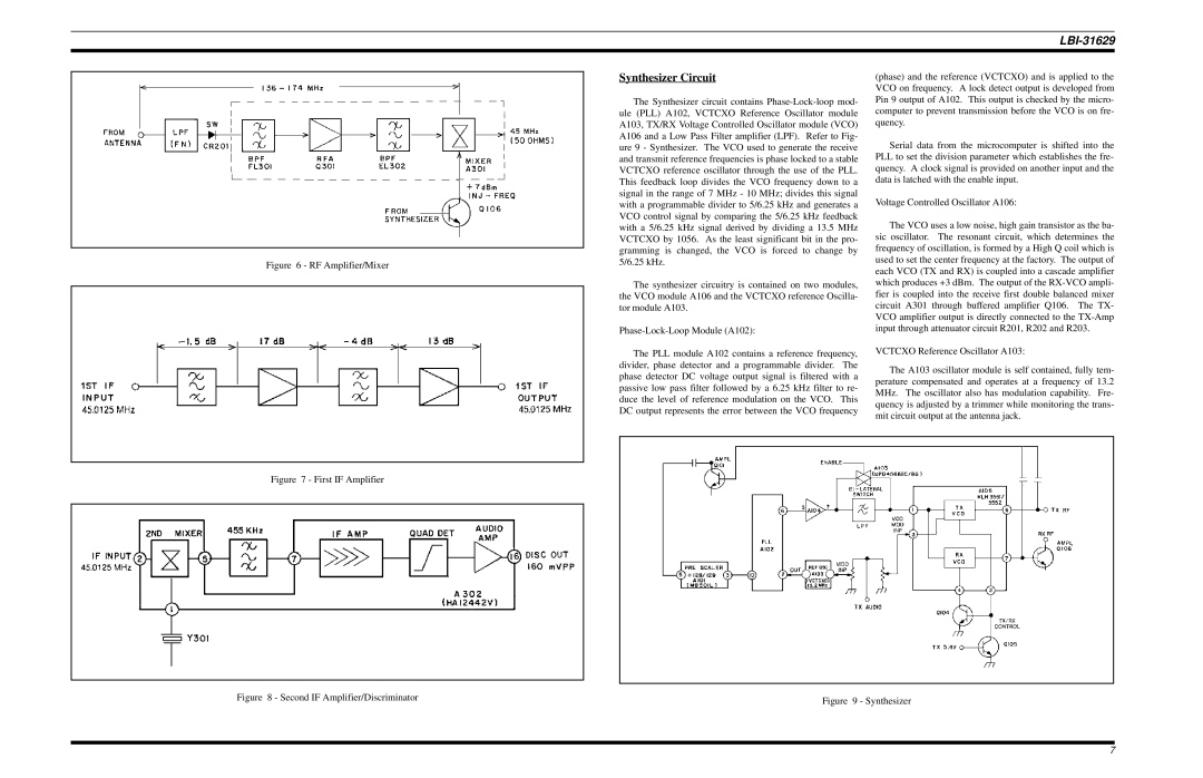
Synthesizer Circuit
The Synthesizer circuit contains
The synthesizer circuitry is contained on two modules, the VCO module A106 and the VCTCXO reference Oscilla- tor module A103.
The PLL module A102 contains a reference frequency, divider, phase detector and a programmable divider. The phase detector DC voltage output signal is filtered with a passive low pass filter followed by a 6.25 kHz filter to re- duce the level of reference modulation on the VCO. This DC output represents the error between the VCO frequency
(phase) and the reference (VCTCXO) and is applied to the VCO on frequency. A lock detect output is developed from Pin 9 output of A102. This output is checked by the micro- computer to prevent transmission before the VCO is on fre- quency.
Serial data from the microcomputer is shifted into the PLL to set the division parameter which establishes the fre- quency. A clock signal is provided on another input and the data is latched with the enable input.
Voltage Controlled Oscillator A106:
The VCO uses a low noise, high gain transistor as the ba- sic oscillator. The resonant circuit, which determines the frequency of oscillation, is formed by a High Q coil which is used to set the center frequency at the factory. The output of each VCO (TX and RX) is coupled into a cascade amplifier which produces +3 dBm. The output of the
VCTCXO Reference Oscillator A103:
The A103 oscillator module is self contained, fully tem- perature compensated and operates at a frequency of 13.2 MHz. The oscillator also has modulation capability. Fre- quency is adjusted by a trimmer while monitoring the trans- mit circuit output at the antenna jack.
Figure 8 - Second IF Amplifier/Discriminator
Figure 9 - Synthesizer
7