nForce 750i SLI Motherboard
 FSB (QDR), MHz
Use the + or – keys to scroll through new values for the CPU FSB frequency or type in a new value. Note that the Actual FSB (QDR) reflects the actual frequency that takes effect on a reboot.
 MEM (DDR), MHz
Use the + or – keys to scroll through new values for the memory frequency or type in a new value. Note that the Actual MEM (DDR) reflects the actual frequency that takes effect when the system reboots.
 Memory Timing Setting
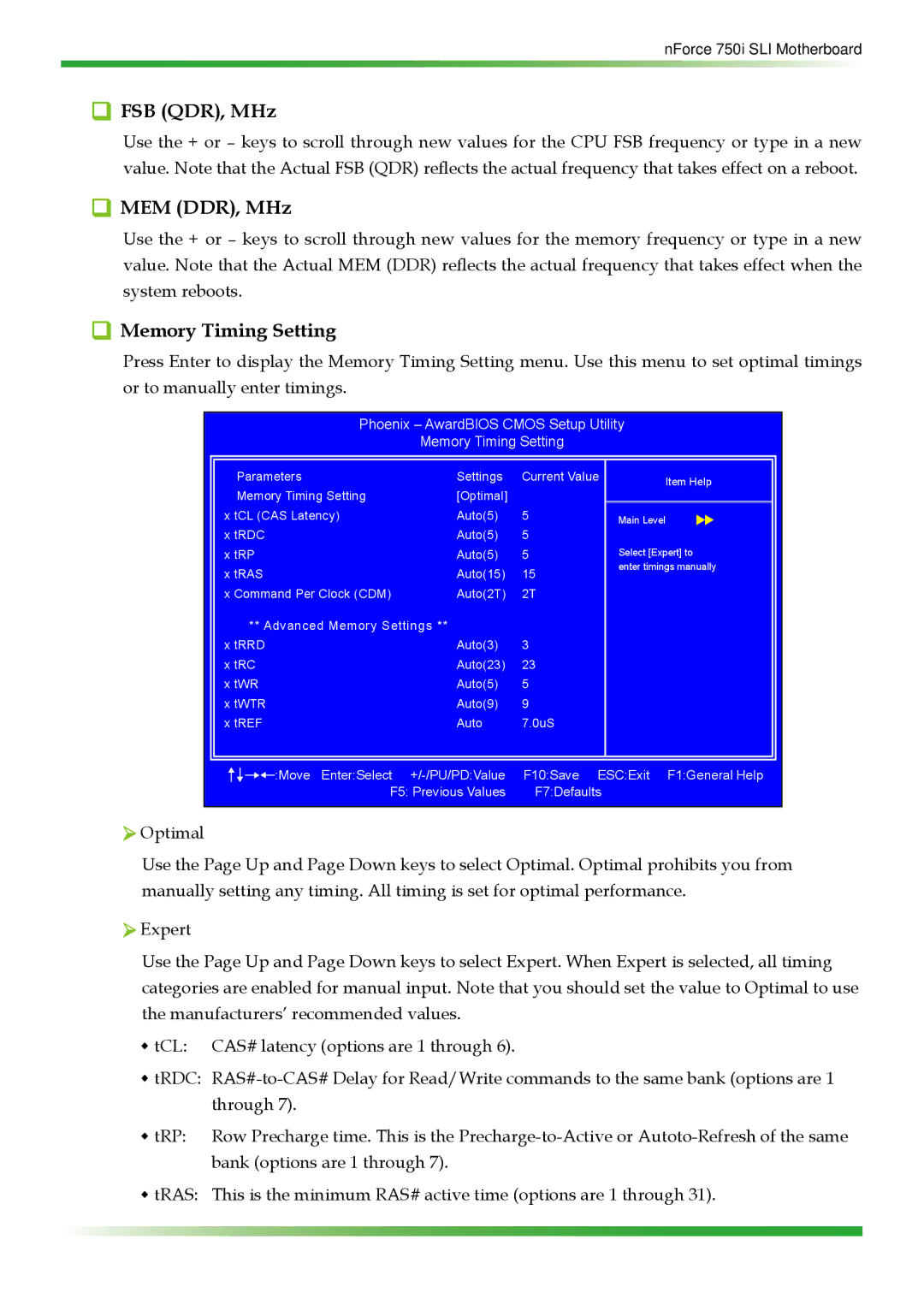
Press Enter to display the Memory Timing Setting menu. Use this menu to set optimal timings or to manually enter timings.
Phoenix – AwardBIOS CMOS Setup Utility
Memory Timing Setting
Parameters | Settings | Current Value |
Memory Timing Setting | [Optimal] |
|
x tCL (CAS Latency) | Auto(5) | 5 |
x tRDC | Auto(5) | 5 |
x tRP | Auto(5) | 5 |
x tRAS | Auto(15) | 15 |
x Command Per Clock (CDM) | Auto(2T) | 2T |
** Advanced Memory Settings ** |
|
|
x tRRD | Auto(3) | 3 |
x tRC | Auto(23) | 23 |
x tWR | Auto(5) | 5 |
x tWTR | Auto(9) | 9 |
x tREF | Auto | 7.0uS |
Item Help
Main Level
Select [Expert] to enter timings manually
:Move Enter:Select | F10:Save ESC:Exit F1:General Help |
F5: Previous Values | F7:Defaults |
![]() Optimal
Optimal
Use the Page Up and Page Down keys to select Optimal. Optimal prohibits you from manually setting any timing. All timing is set for optimal performance.
![]() Expert
Expert
Use the Page Up and Page Down keys to select Expert. When Expert is selected, all timing categories are enabled for manual input. Note that you should set the value to Optimal to use the manufacturers’ recommended values.
wtCL: CAS# latency (options are 1 through 6).
wtRDC:
wtRP: Row Precharge time. This is the
wtRAS: This is the minimum RAS# active time (options are 1 through 31).
