www.fairchildsemi.com
Since the output current is being controlled instead of the output voltage, the output voltage will actually vary with the number of LEDs on the output. The same applies to the auxiliary winding that provides the bias supply to the FAN7554D. Consequently, the transformer had to be designed to provide enough bias when powering one LED. Then when powering three LEDs, the bias voltage is significantly higher. In order to maintain reliable operation, a regulator circuit consisting of R20, ZD1 and Q3 is implemented. This circuit will regulate the voltage to the Vcc pin of the FAN7554 to 18V when there are multiple LEDs on the output. Please note that this circuit would not be needed in a conventional application where the number of LEDs on the output is known and fixed. In such an application, the transformer would then be designed to provide the required Vcc voltage for that particular number of LEDs.
The FAN7554D will take feedback information from the sense resistor, R12, and from the feedback pin, pin 1, and generate a PWM signal that is applied to the FET at location Q1. This FET, FDQ2N80, is a 2A, 800V,
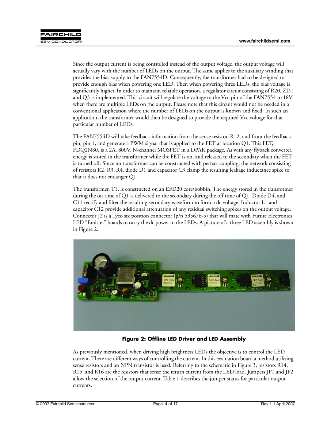
The transformer, T1, is constructed on an EFD20 core/bobbin. The energy stored in the transformer during the on time of Q1 is delivered to the secondary during the off time of Q1. Diode D4, and C11 rectify and filter the resulting secondary waveform to form a dc voltage. Inductor L1 and capacitor C12 provide additional attenuation of any residual switching spikes on the output voltage. Connector J2 is a Tyco six position connector (p/n
Figure 2: Offline LED Driver and LED Assembly
As previously mentioned, when driving high brightness LEDs the objective is to control the LED current. There are different ways of controlling the current. In this evaluation board a method utilizing sense resistors and an NPN transistor is used. Referring to the schematic in Figure 3, resistors R14, R15, and R16 are the resistors that sense the return current from the LED load. Jumpers JP1 and JP2 allow the selection of the output current. Table 1 describes the jumper status for particular output currents.
© 2007 Fairchild Semiconductor | Page 4 of 17 | Rev 1.1 April 2007 |
