MB15E07SL
■PIN DESCRIPTIONS
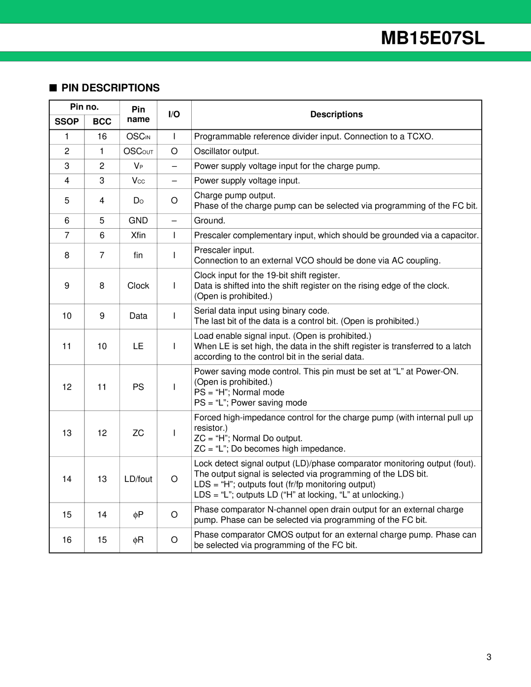
Pin no. | Pin | I/O | Descriptions | ||
|
| ||||
SSOP | BCC | name | |||
|
| ||||
|
|
| |||
|
|
|
|
| |
1 | 16 | OSCIN | I | Programmable reference divider input. Connection to a TCXO. | |
|
|
|
|
| |
2 | 1 | OSCOUT | O | Oscillator output. | |
|
|
|
|
| |
3 | 2 | VP | – | Power supply voltage input for the charge pump. | |
|
|
|
|
| |
4 | 3 | VCC | – | Power supply voltage input. | |
|
|
|
|
| |
5 | 4 | DO | O | Charge pump output. | |
Phase of the charge pump can be selected via programming of the FC bit. | |||||
|
|
|
| ||
|
|
|
|
| |
6 | 5 | GND | – | Ground. | |
|
|
|
|
| |
7 | 6 | Xfin | I | Prescaler complementary input, which should be grounded via a capacitor. | |
|
|
|
|
| |
8 | 7 | fin | I | Prescaler input. | |
Connection to an external VCO should be done via AC coupling. | |||||
|
|
|
| ||
|
|
|
|
| |
|
|
|
| Clock input for the | |
9 | 8 | Clock | I | Data is shifted into the shift register on the rising edge of the clock. | |
|
|
|
| (Open is prohibited.) | |
|
|
|
|
| |
10 | 9 | Data | I | Serial data input using binary code. | |
The last bit of the data is a control bit. (Open is prohibited.) | |||||
|
|
|
| ||
|
|
|
|
| |
|
|
|
| Load enable signal input. (Open is prohibited.) | |
11 | 10 | LE | I | When LE is set high, the data in the shift register is transferred to a latch | |
|
|
|
| according to the control bit in the serial data. | |
|
|
|
|
| |
|
|
|
| Power saving mode control. This pin must be set at “L” at | |
12 | 11 | PS | I | (Open is prohibited.) | |
PS = “H”; Normal mode | |||||
|
|
|
| ||
|
|
|
| PS = “L”; Power saving mode | |
|
|
|
|
| |
|
|
|
| Forced | |
13 | 12 | ZC | I | resistor.) | |
ZC = “H”; Normal Do output. | |||||
|
|
|
| ||
|
|
|
| ZC = “L”; Do becomes high impedance. | |
|
|
|
|
| |
|
|
|
| Lock detect signal output (LD)/phase comparator monitoring output (fout). | |
14 | 13 | LD/fout | O | The output signal is selected via programming of the LDS bit. | |
LDS = “H”; outputs fout (fr/fp monitoring output) | |||||
|
|
|
| ||
|
|
|
| LDS = “L”; outputs LD (“H” at locking, “L” at unlocking.) | |
|
|
|
|
| |
15 | 14 | φP | O | Phase comparator | |
pump. Phase can be selected via programming of the FC bit. | |||||
|
|
|
| ||
|
|
|
|
| |
16 | 15 | φR | O | Phase comparator CMOS output for an external charge pump. Phase can | |
be selected via programming of the FC bit. | |||||
|
|
|
| ||
|
|
|
|
| |
3