
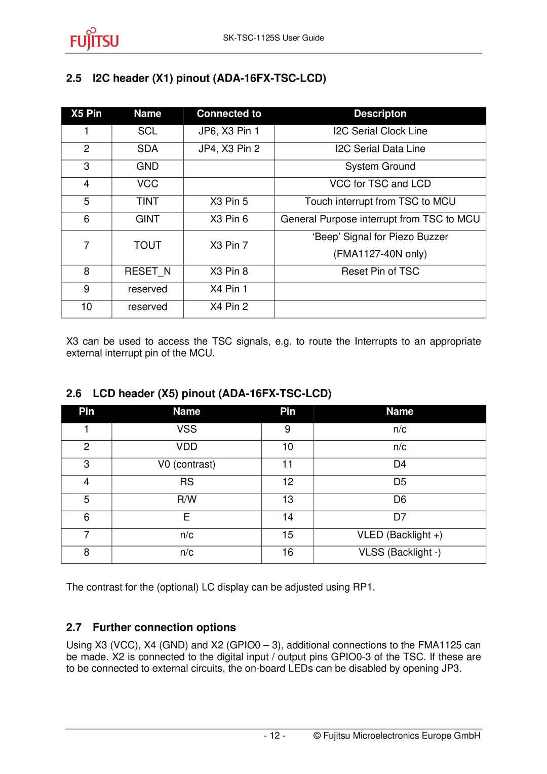
SK-TSC-1125S specifications
Fujitsu's SK-TSC-1125S is an advanced storage solution designed to meet the increasing demands of data management in modern businesses. This device stands out due to its high reliability, impressive performance, and cutting-edge technology. Engineered for efficiency, the SK-TSC-1125S is especially suitable for both enterprise-level applications and small to medium-sized businesses that require robust data handling capabilities.One of the key features of the SK-TSC-1125S is its high-capacity storage. With up to 12TB of data capacity, this storage solution caters to the needs of organizations dealing with vast amounts of information. This scale of storage allows for greater flexibility in managing large databases, virtual environments, and extensive backup solutions, ensuring that businesses can maintain efficient operations without encountering storage bottlenecks.
Additionally, the SK-TSC-1125S utilizes advanced data protection features, including RAID configurations. These configurations enhance data availability and redundancy, protecting against hardware failures. The ability to switch between various RAID levels provides versatility for different data protection needs, making it adaptable to various business requirements.
The performance of the SK-TSC-1125S is further enhanced by its use of high-speed interface technologies. Supporting USB 3.0 and other high-throughput connectivity options, this device ensures rapid data transfer speeds, significantly reducing the time to back up or retrieve critical information. This speed is vital for organizations looking to streamline their workflows and enhance productivity.
In terms of energy efficiency, the SK-TSC-1125S incorporates power-saving technologies that help reduce operational costs. With features like automatic power management and low power consumption during idle states, this storage solution aligns with modern sustainability initiatives, making it an eco-friendly choice for businesses.
Moreover, Fujitsu emphasizes user-friendly features, including intuitive management software that allows users to monitor performance, conduct health checks, and manage configurations with ease. This simplification of management processes translates into reduced downtime and more efficient resource allocation.
In conclusion, Fujitsu’s SK-TSC-1125S is a compelling storage solution that combines high capacity, reliability, performance, and energy efficiency. With its advanced technologies and robust features, it is well-equipped to address the diverse data management needs of contemporary enterprises, paving the way for effective data utilization and strategic business growth. As organizations increasingly rely on data-driven decision-making, solutions like the SK-TSC-1125S stand ready to support their journey toward digital transformation.