LCD TV Service Manual
4. Chassis Layout and Overall Wiring Diagrams
Boards and Chassis Layout
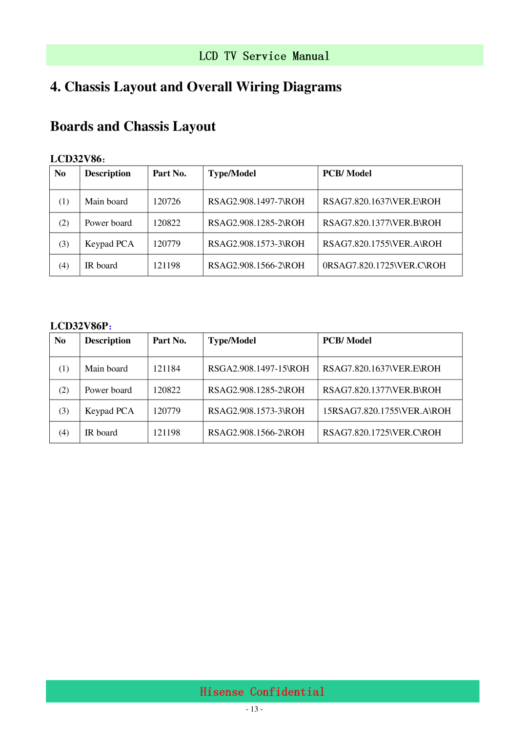
LCD32V86:
No | Description | Part No. | Type/Model | PCB/ Model |
|
|
|
|
|
(1) | Main board | 120726 | RSAG7.820.1637\VER.E\ROH | |
|
|
|
|
|
(2) | Power board | 120822 | RSAG7.820.1377\VER.B\ROH | |
|
|
|
|
|
(3) | Keypad PCA | 120779 | RSAG7.820.1755\VER.A\ROH | |
|
|
|
|
|
(4) | IR board | 121198 | 0RSAG7.820.1725\VER.C\ROH | |
|
|
|
|
|
LCD32V86P:
No | Description | Part No. | Type/Model | PCB/ Model |
|
|
|
|
|
(1) | Main board | 121184 | RSAG7.820.1637\VER.E\ROH | |
|
|
|
|
|
(2) | Power board | 120822 | RSAG7.820.1377\VER.B\ROH | |
|
|
|
|
|
(3) | Keypad PCA | 120779 | 15RSAG7.820.1755\VER.A\ROH | |
|
|
|
|
|
(4) | IR board | 121198 | RSAG7.820.1725\VER.C\ROH | |
|
|
|
|
|
Hisense Confidential
- 13 -
