Floating | Floating | Fixed | Fixed | Fixed | LD/ST | LD/ST |
Point | Point | Point | Point | Point | Unit | Unit |
Unit | Unit | Unit | Unit | Unit |
|
|
FPU1 | FPU2 | FXU1 | FXU2 | FXU3 | LS1 | LS2 |
Branch/Dispatch | Branch history table 2048 entries |
|
| |||
|
| Branch target cache 256 entries |
|
| ||
| 32 KB, | 64 KB, |
|
| ||
| Memory Mgmt Unit |
| Memory Mgmt Unit |
| ||||
| Instruction Cache |
|
| Data Cache |
| |||
|
| IU |
| DU |
| |||
|
|
|
|
|
|
|
|
|
|
|
| 32 |
|
|
| 32 |
|
|
|
| Bytes |
|
| Bytes | ||
|
|
|
|
|
|
|
| |
| BIU |
| Bus Interface Unit L2 Control, Clock |
| ||||
|
|
|
|
|
|
|
|
|
|
|
|
|
|
|
|
|
|
CPU registers:
32 x
32 x
Register buffers for register renaming: 24 FP
16 Integer
Direct Mapped
32 Bytes
@ 200 MHz=6.4 GB/s
L2 Cache
4 MB
16 Bytes |
@ 100 MHz=1.6 GB/s |
6XX Bus |
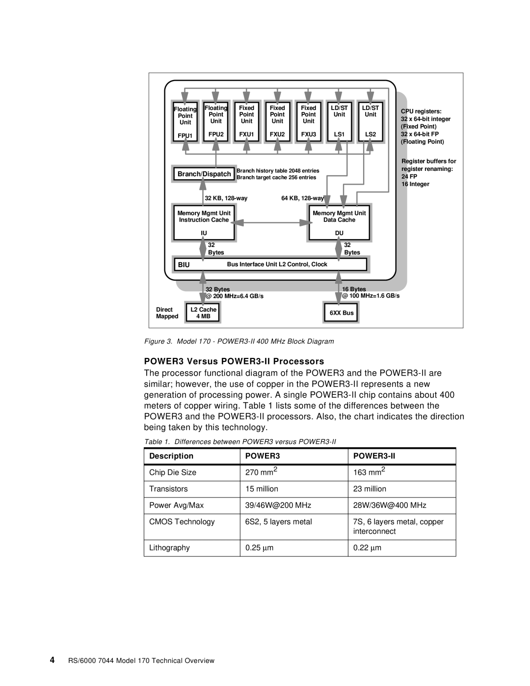
Figure 3. Model 170 - POWER3-II 400 MHz Block Diagram
POWER3 Versus POWER3-II Processors
The processor functional diagram of the POWER3 and the
Table 1. Differences between POWER3 versus
Description | POWER3 |
|
|
|
|
Chip Die Size | 270 mm2 | 163 mm2 |
Transistors | 15 million | 23 million |
|
|
|
Power Avg/Max | 39/46W@200 MHz | 28W/36W@400 MHz |
|
|
|
CMOS Technology | 6S2, 5 layers metal | 7S, 6 layers metal, copper |
|
| interconnect |
|
|
|
Lithography | 0.25 μm | 0.22 μm |
|
|
|