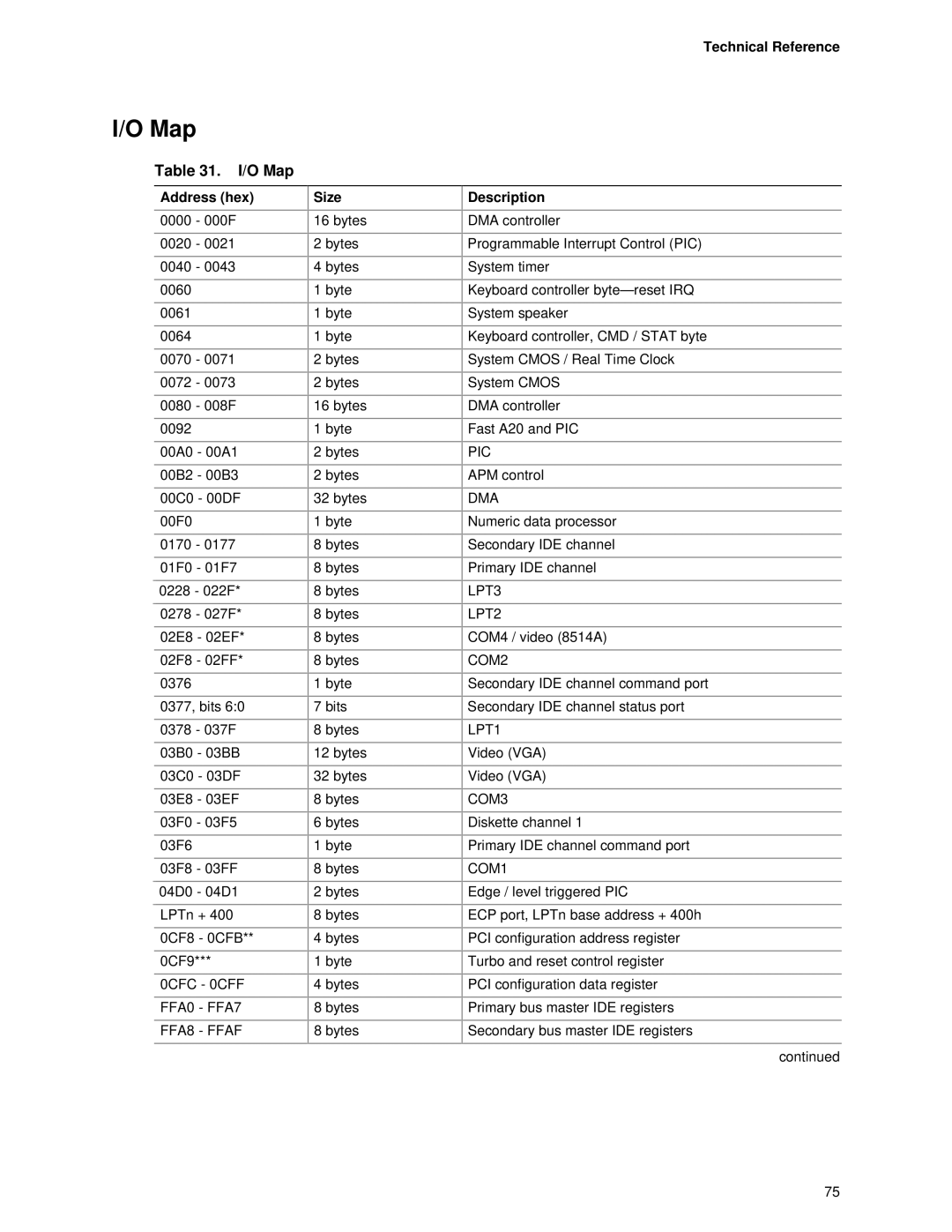
D845HV, D845WN specifications
The Intel D845WN and D845HV motherboards have garnered attention for their robust features and reliability, making them suitable choices for a range of computing needs. Both motherboards belong to Intel’s 845 chipset family, which was designed to support the Pentium 4 processors, providing a foundation for both performance and value.The Intel D845WN motherboard is recognized for its standard ATX form factor, which allows for versatility in case selection and expands the options for build configurations. It supports the Pentium 4 processors with a socket 478 interface, accommodating speeds of 1.3 GHz to 3.0 GHz. This motherboard is equipped with a front-side bus (FSB) speed of 400/533 MHz, ensuring fast data transfer rates between the processor and other components.
On the memory side, the D845WN supports up to 2 GB of DDR SDRAM, making it compatible with a range of memory options for efficient multitasking and improved performance. It features two memory slots for Dual Channel DDR support, enhancing memory bandwidth. The onboard graphics capabilities are powered by Intel's integrated graphics, making the D845WN capable of basic graphical tasks without requiring a dedicated graphics card, ideal for general computing or light gaming.
In contrast, the D845HV model shares many similarities with the D845WN but emphasizes additional features that cater to more advanced users. It includes support for Intel's RAID technology, allowing users to set up mirrored or striped disk configurations for improved data redundancy and performance. Furthermore, the D845HV motherboard comes with more extensive expansion slots, including additional PCI and an AGP slot for dedicated graphics cards, enhancing its overall upgradeability.
Both motherboards include integrated audio capabilities courtesy of Intel’s AC'97 Audio technology, ensuring satisfactory sound output for everyday multimedia use. Networking is facilitated through integrated Ethernet support, enabling reliable internet connectivity without needing additional network cards.
In terms of expansion and connectivity, both models feature USB ports, allowing users to connect multiple peripherals effortlessly. The combination of legacy and contemporary interfaces on the D845WN and D845HV ensures compatibility with a wide range of devices and peripherals.
In summary, the Intel D845WN and D845HV motherboards epitomize value-driven performance, offering essential features that cater to a variety of users, from casual computer users to more demanding applications. With their solid build quality and Intel's backing, these motherboards continue to be appreciated even in today's evolving computing landscape.

