4.5 Block Diagram
| CN1 | CN2 | JP16 | JP17 | CN8 Connector with R/C filter | |
|
|
|
|
| ||
|
|
|
|
|
| |
Analog input |
|
|
|
| AMP | 16 channel Multiplexer |
|
|
|
|
|
| |
|
|
|
|
|
| VR1 |
|
|
|
|
|
| CJC |
|
|
| Dip Switch | Control |
| |
CN3 | CN4 |
|
|
| ||
|
| Logic |
| |||
|
|
|
| VR2 | ||
D/O control signal |
|
|
|
|
| |
|
|
|
|
|
| |
|
|
|
|
| CN6 Connector with R/C filter | |
|
|
|
| |||
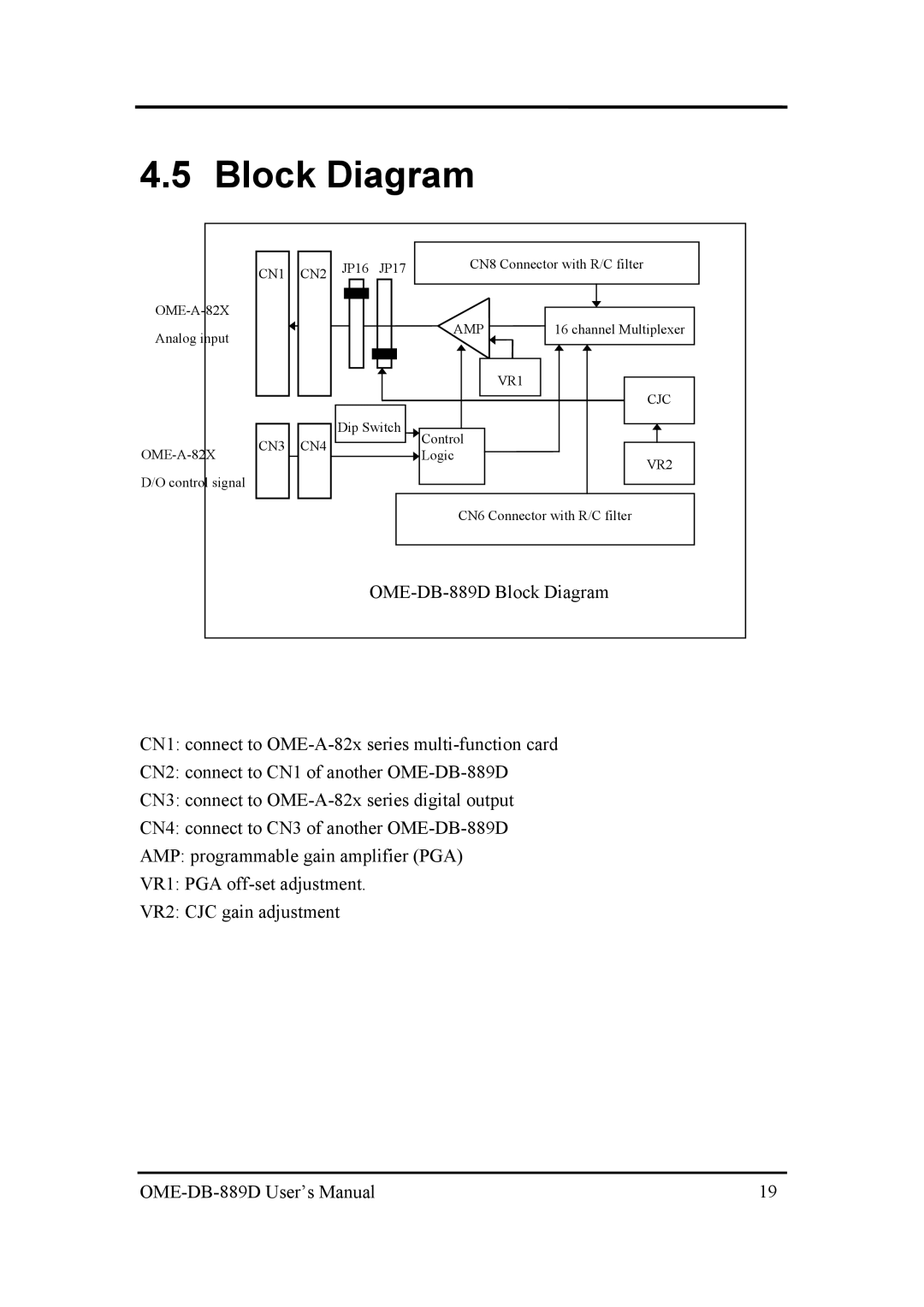
CN1: connect to
CN2: connect to CN1 of another
CN3: connect to
CN4: connect to CN3 of another
AMP: programmable gain amplifier (PGA)
VR1: PGA
VR2: CJC gain adjustment
| 19 |
