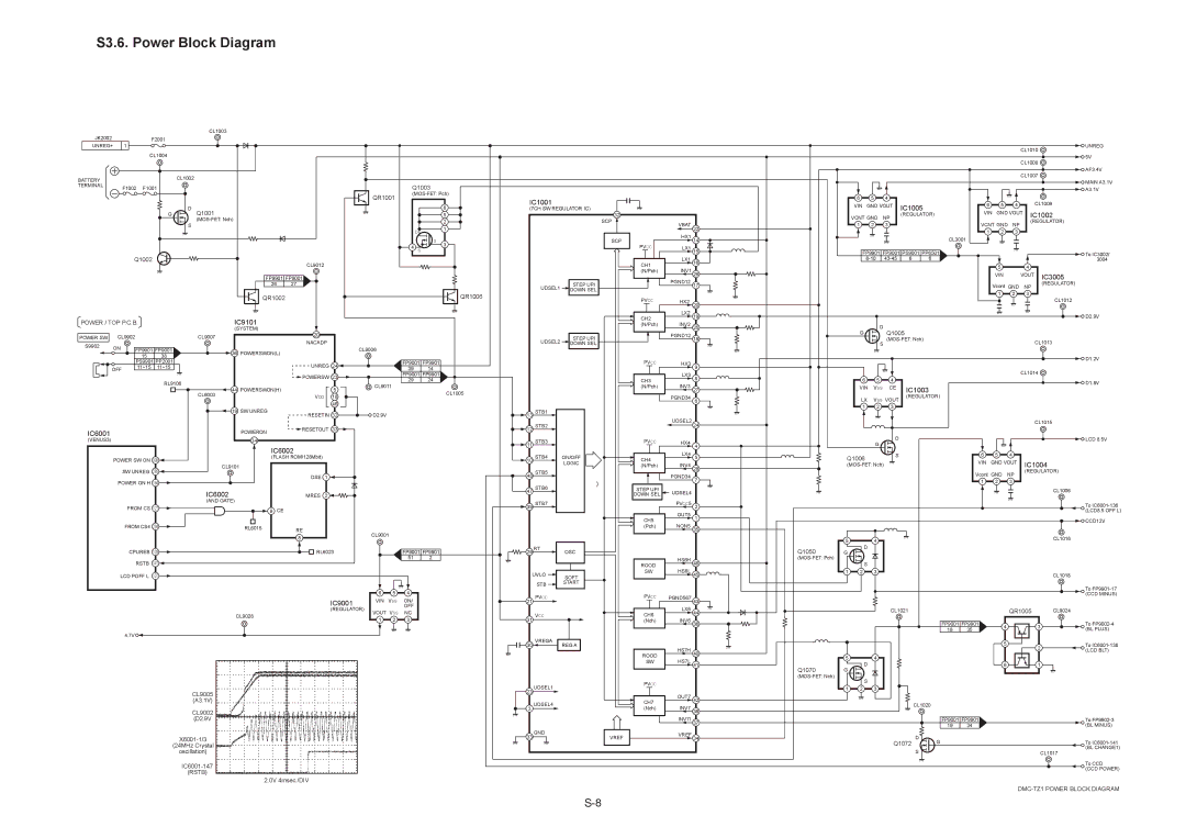
S3.6. Power Block Diagram


CL1003


JK2002


F2001


UNREG+

1


CL1010

UNREG


CL1004


CL1008

5V


CL1007

AF3.4V

BATTERY


CL1002


MAIN A3.1V

TERMINAL


F1002

F1001


Q1003


A3.1V


QR1001

(MOS-FET: Pch)


6


5

4


IC1001


CL1009


D


6


VIN GND VOUT

IC1005


6

5

4


Q1001


(7CH SW REGULATOR IC)


IC1002


G


5


32


VCNT GND NP

(REGULATOR)

VIN

GND VOUT


(MOS-FET: Nch)


2


SCP


(REGULATOR)


S


VBAT 22

1


2

3


VCNT GND

NP


D

1


HX1 14


1

2

3


G

3


SCP


CL3001


4

S


PVCC

LX1


15


FP9901 FP9001 PS9001 PP6501


To IC3002/


Q1002


CL9012


CH1

LX1 16


8-10

43-45

6

6


3004


5


4


(N/Pch)

INV1 26


FP9901 FP9001


VIN

VOUT

IC3005


26

27


UDSEL1

STEP UP/


PGND12 17


Vcont GND

NP

(REGULATOR)


QR1006

DOWN SEL.


1

2

3


QR1002


PVCC


CL1012


HX2


20


POWER / TOP P.C.B.


IC9101


CH2

LX2 19


D2.9V


(N/Pch)

INV2

25


D


(SYSTEM)

20


G

Q1005


POWER SW

CL9902


CL9007


STEP UP/


PGND12 18


UDSEL2


S

(MOS-FET: Nch)


CL1013

S9902

ON


NACADP


DOWN SEL.


FP9901 FP9001


CL9006


36 POWERSWON(L)


15

38


D1.2V


PS9901 PP2001


FP9001 FP9901


PVCC

HX3


UNREG 24


OFF


11~15

11~15


39

14


9


LX3


CL1014


POWERSW 23


FP9001 FP9901


8


RL9106


29

24


CH3


6

5

4


D1.8V


CL9011


INV3


44 POWERSWON(H)


5


(N/Pch)

27


VIN

VSS

CE

IC1003


CL1005


CL6003

VDD

18


PGND34

6


LX

VSS

VOUT

(REGULATOR)


46


1

2

3


19 SW UNREG


13 STB1


RESETIN 32

D2.9V


UDSEL2


12 STB2


24


CL1015

IC6001


POWERON

RESETOUT 33


D


LCD 8.5V

(VENUS3)


34


11 STB3


PVCC

HX4

4


G


IC6002


LX4


S


6


5

4


POWER SW ON 308


(FLASH ROM/128Mbit)


10 STB4

ON/OFF

CH4

5

Q1006


VIN

GND VOUT


CL9101


LOGIC

(N/Pch)

INV4

28

(MOS-FET: Nch)


IC1004


SW UNREG 285


DSE

1


48 STB5


PGND34


Vcont GND NP

(REGULATOR)


7


POWER ON H 194


)


1


2

3


47 STB6

STEP UP/


CL1006


IC6002

MRES

2


UDSEL4


DOWN SEL.


(AND GATE)


39 STB7


PVCC5

2


To IC6001-136


FROM CS

127


9 CE


OUT5


(LCD8.5 OFF L)


CH5

1


CCD12V


NON5 35


FROM CS4 204


RL6015

RE


CL9001


(Pch)


8


5


4


CL1016


D


CPUREB 129


RL6023


FP9001 FP9901


29 RT

OSC


Q1050

G


51

2


HS6H

(MOS-FET: Pch)


RSTB 147


ROOD

46


S


LCD POFF L

137


UVLO

SOFT

SW

HS6L 45

1

2

3


CL1018


STB

START


To FP9901-17


6

5

4


21 PVCC


PVCC

PGND567 43


(CCD MINUS)


IC9001

VIN

VSS

ON/


OFF


LX6 44


QR1005


CL9028


(REGULATOR)

VOUT VSS

NC


31 VCC


CH6


CL1021


CL9024


1

2

3


(Nch)

INV6 36


FP9001 FP9901


4


3

To FP9002-4


18

35


(BL PLUS)


4.7V


30 VREGA


REG A


HS7H 40


5


2

To IC6001-138


(LCD BLT)


ROOD

5


4


HS7L


SW


D


41


6


1


Q1070

G


(MOS-FET: Nch)


S


UDSEL1


PVCC


1

2

3


CL9005


23


OUT7 42


(A3.1V)


3 UDSEL4


CH7


CL1020


CL9002


(Nch)

INV7

38


(D2.9V


INV7I 37


FP9001 FP9901


To FP9902-3


19

34


(BL MINUS)


X6001-1/3


33 GND


VREF

VREF 34


D

G


To IC6001-141


(24MHz Crystal


Q1072


(BL CHANGE1)


oscillation)


S


CL1017


IC6001-147


To CCD


(CCD POWER)


(RSTB)


2.0V 4msec./DIV


DMC-TZ1 POWER BLOCK DIAGRAM

S-8

Page 40
Image 40
Panasonic DMC-TZ1GC, DMC-TZ1SG, DMC-TZ1PP, DMC-TZ1PL, DMC-TZ1GT, DMC-TZ1EF, DMC-TZ1EE manual S3.6. Power Block Diagram, IC1002

DMC-TZ1EF, DMC-TZ1EG, DMC-TZ1GN, DMC-TZ1EB, DMC-TZ1EGM-K specifications

The Panasonic DMC-TZ1 series represents a significant milestone in the realm of compact digital cameras. Designed with user-friendliness and advanced technology in mind, these models, including the DMC-TZ1PL, DMC-TZ1GC, DMC-TZ1EE, DMC-TZ1SG, and DMC-TZ1PP, cater to both amateur photographers and enthusiasts alike.

One of the standout features of the DMC-TZ1 series is its impressive 10x optical zoom lens. This capability allows users to capture stunning imagery with versatility, from wide landscapes to detailed close-ups. The lens is paired with a 7.2-megapixel sensor, which ensures sharp and vivid images, suitable for printing and sharing.

Incorporating Panasonic’s advanced image stabilization technology, the DMC-TZ1 models reduce the effects of camera shake, making them ideal for handheld shooting, especially in low-light conditions. This feature is particularly useful for travel photography, as it enables users to capture steady shots without the need for bulky tripods.

The TZ1 series is equipped with several automatic shooting modes, including portrait, landscape, and night scene settings. This intelligent scene selection enhances image quality, allowing photographers to focus on composition rather than technical settings. The integration of ISO sensitivity adjustments further contributes to the camera's performance in challenging lighting scenarios.

The cameras also feature a bright 2.5-inch LCD screen, offering a clear view for framing shots and reviewing images. Its user-friendly interface makes navigation simple, ensuring that users can easily adjust settings or browse through their images.

Additionally, the DMC-TZ1 series supports various imaging formats, including JPEG and AVCHD Lite for video recording, allowing for versatility in media storage. High-definition video recording capability opens the door for stunning video capture, complementing the already robust still photography features.

Powered by a rechargeable lithium-ion battery, the TZ1 models promise extended shooting sessions, perfect for vacations and events. Their compact design means they can easily slip into pockets or bags, making them convenient companions for photographers on the go.

In summary, the Panasonic DMC-TZ1PL, DMC-TZ1GC, DMC-TZ1EE, DMC-TZ1SG, and DMC-TZ1PP embody the ideal blend of portability, advanced imaging technology, and user-centered design. They make photography accessible, encouraging users to capture memories in exceptional detail, whether in daily life or during adventurous travels.