Philips Semiconductors | Product data | ||
|
|
| |
|
|
| |
CBT6800 | |||
for live insertion | |||
|
| ||
|
|
| |
|
|
| |
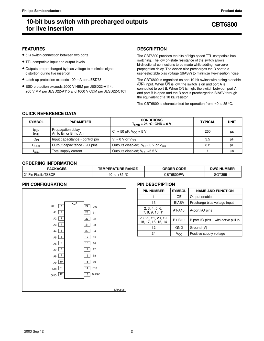
FEATURES
•5 Ω switch connection between two ports
•TTL compatible input and output levels
•Outputs are precharged by bias voltage to minimize signal distortion during live insertion
DESCRIPTION
The CBT6800 provides ten bits of
•
•
ESD protection exceeds 2000 V HBM per
200 V MM per
The CBT6800 is organized as one
The CBT6800 is characterized for operation from
QUICK REFERENCE DATA
SYMBOL | PARAMETER | CONDITIONS | TYPICAL | UNIT | |
Tamb = 25 °C; GND = 0 V | |||||
|
|
|
| ||
tPLH | Propagation delay | CL = 50 pF; VCC = 5 V | 250 | ps | |
tPHL | An to Bn or Bn to An | ||||
|
|
| |||
CIN | Input capacitance - control pin | VI = 0 V or VCC | 3.5 | pF | |
COUT | Output capacitance - I/O pins | Outputs disabled; VO = 0 V or VCC | 8.2 | pF | |
ICCZ | Total supply current | Outputs disabled; VCC =5.5 V | 1 | ∝A |
ORDERING INFORMATION
PACKAGES | TEMPERATURE RANGE | ORDER CODE | DWG NUMBER |
|
|
|
|
CBT6800PW |
PIN CONFIGURATION
|
|
|
|
|
|
OE | 1 |
| 24 | Vcc | |
|
|
|
|
|
|
A1 | 2 |
| 23 | B1 | |
|
|
|
|
|
|
A2 | 3 |
| 22 | B2 | |
|
|
|
|
|
|
A3 | 4 |
| 21 | B3 | |
|
|
|
|
|
|
A4 | 5 |
| 20 | B4 | |
|
|
|
|
|
|
A5 | 6 |
| 19 | B5 | |
|
|
|
|
|
|
A6 | 7 |
| 18 | B6 | |
|
|
|
|
|
|
A7 | 8 |
| 17 | B7 | |
|
|
|
|
|
|
A8 | 9 |
| 16 | B8 | |
|
|
|
| ||
|
|
|
|
|
|
A9 | 10 |
| 15 | B9 | |
|
|
|
|
|
|
A10 | 11 |
| 14 | B10 | |
|
|
|
|
|
|
GND | 12 |
| 13 | BIASV | |
|
|
|
|
|
|
PIN DESCRIPTION
PIN NUMBER | SYMBOL | NAME AND FUNCTION | |||
|
|
|
|
| |
1 |
|
|
| Output enable | |
| OE | ||||
13 | BIASV | Precharge bias voltage input | |||
|
|
|
|
| |
2, 3, 4, 5, 6, | |||||
7, 8, 9, 10, 11 | |||||
|
|
|
| ||
|
|
|
|
| |
23, 22, 21, 20, 19, | |||||
18, 17, 16, 15, 14 | |||||
|
|
|
| ||
|
|
| |||
12 | GND | Ground (V) | |||
|
|
| |||
24 | VCC | Positive supply voltage | |||
SA00505
2003 Sep 12 | 2 |
