
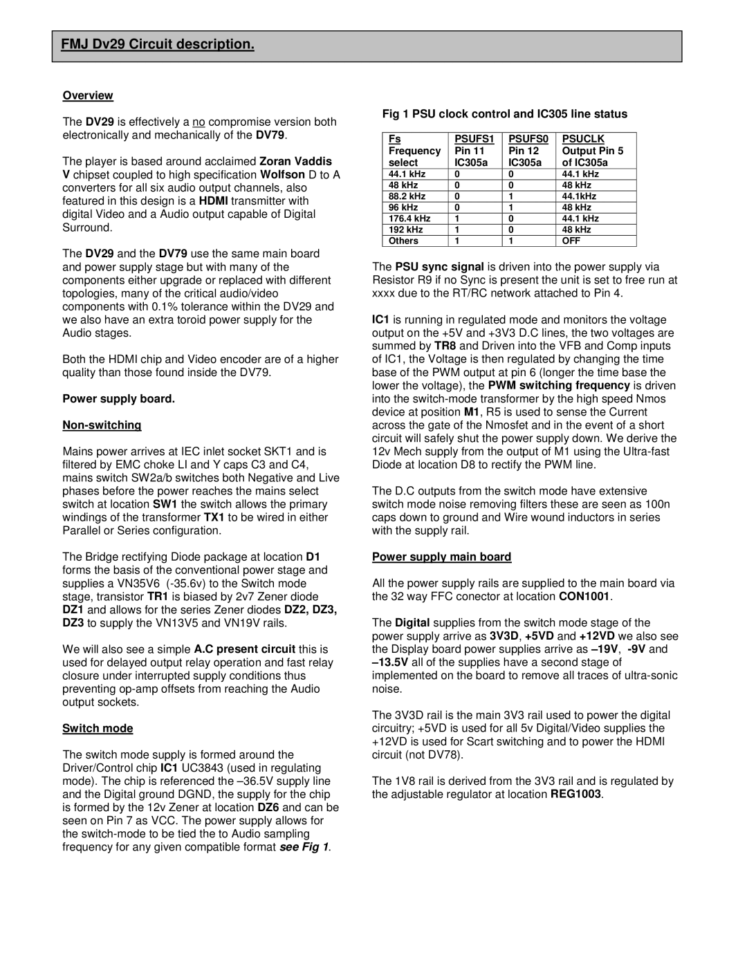
DV29 specifications
The Philips DV29 is a versatile DVD player that reflects the brand's commitment to delivering high-quality entertainment solutions. This model is designed to cater to the needs of users who seek an optimal viewing experience while enjoying their favorite movies and shows. With a sleek and compact design, the DV29 fits seamlessly into any home entertainment setup.One of the standout features of the Philips DV29 is its compatibility with various disc formats. The player can handle not just standard DVDs but also CD-RW, CD-R, and MP3-CD formats, making it a versatile choice for media playback. This broad compatibility ensures that users can enjoy a vast library of content without the need for multiple devices. Additionally, the player supports multiple audio formats, including Dolby Digital and DTS, which enhances the audio experience significantly, providing a theater-like experience right at home.
The Philips DV29 incorporates advanced video technologies to enhance the quality of playback. With an 8-bit video DAC, this player offers improved color depth and clarity, ensuring that even standard-definition content appears sharp and vibrant. The model also features progressive scan functionality, which allows for smoother motion and crisper images, making it an excellent choice for those who want to get the most out of their DVDs.
Another noteworthy characteristic of the Philips DV29 is its user-friendly interface. Navigating through menus and options is straightforward, thanks to its well-designed remote control and on-screen display. This ease of use makes it accessible for all age groups, from tech-savvy individuals to those less familiar with modern gadgets.
Furthermore, the Philips DV29 is equipped with a range of connectivity options. It comes with composite and S-Video outputs, allowing users to connect the player to different types of TVs and audiovisual equipment easily. Its compact design ensures that it can be easily integrated into any media setup without consuming too much space.
In summary, the Philips DV29 is a well-rounded DVD player that offers a great combination of versatility, quality, and user-friendliness. Its range of supported formats, advanced video technologies, and thoughtful design characteristics make it an excellent addition to any home entertainment system. Whether for family movie nights or solo viewing experiences, the DV29 is equipped to deliver a satisfying audiovisual journey.