TDA6107JF specifications
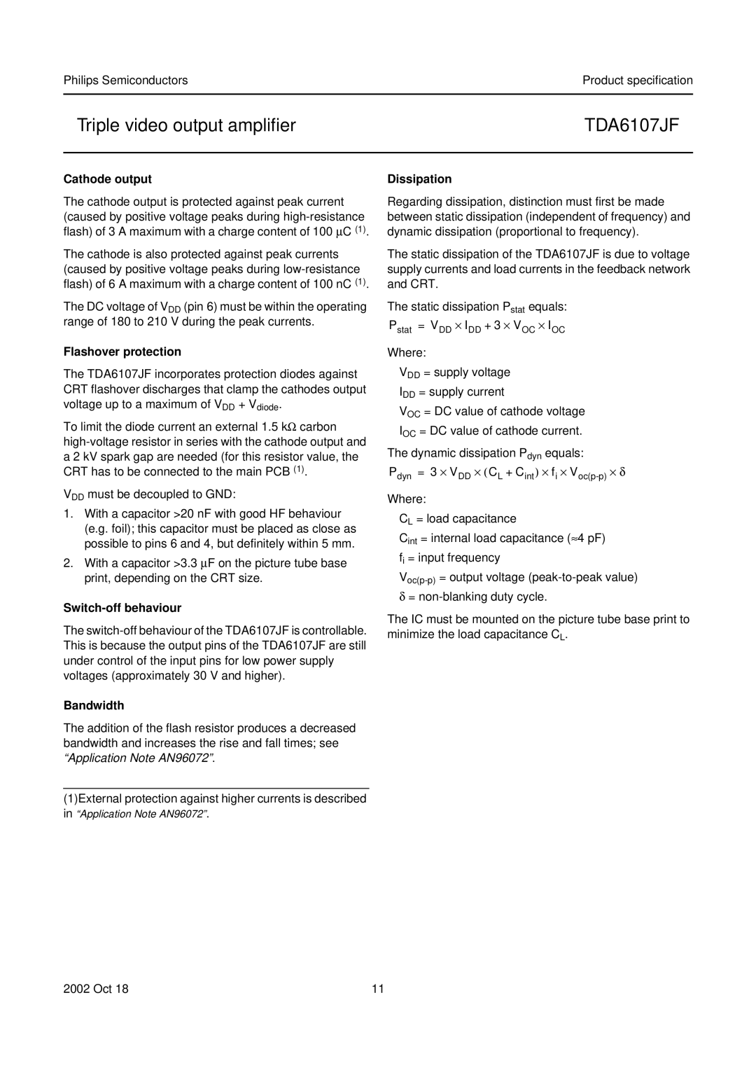
The Philips TDA6107JF is a state-of-the-art video output integrated circuit (IC) designed for use in various consumer and professional electronics. It's particularly popular in television applications and display systems, showcasing advanced features that enhance image quality and performance.One of the main features of the TDA6107JF is its ability to handle RGB video signals with exceptional fidelity. It supports a wide range of signal input levels, which makes it versatile for different types of video data. This allows devices using the IC to achieve vibrant colors and clear images, appealing to both casual viewers and professionals who demand high-quality video output.
The TDA6107JF incorporates sophisticated technologies including built-in amplification, enabling users to drive the display directly without needing additional external components. This integration simplifies circuit design, reducing the overall component count and potential points of failure within a system. As a result, manufacturers can create more compact and cost-effective designs while still delivering high performance.
In terms of characteristics, the TDA6107JF is distinguished by its low power consumption, which is essential for battery-operated devices. Enhanced efficiency also leads to reduced heat generation, ensuring longevity and reliability in performance. It operates over a wide voltage range, making it compatible with various power supply systems, which further broadens its applications.
Moreover, the TDA6107JF boasts excellent linearity and low distortion, which is crucial for maintaining the integrity of video signals during processing. This precision results in a clearer image with fewer artifacts, thereby enhancing the overall viewing experience.
Additionally, the TDA6107JF is equipped with features such as color burst extraction and adjustable gain settings, providing flexibility for different use cases. This means that manufacturers can tailor their devices to meet specific market needs or consumer preferences.
Overall, the Philips TDA6107JF represents a significant advancement in video output technology, merging functionality and performance in a single package. Its combination of features, efficiency, and reliability makes it an essential component in the world of display technology, underpinning its widespread adoption in modern electronic devices. As video and display standards evolve, the TDA6107JF continues to be a relevant and essential player in this competitive landscape.
